Automatic gain control amplifier for canceling direct current offset

An automatic gain control and gain amplifier technology, applied in gain control, amplification control, electrical components, etc., can solve the problems of large loss of low-frequency signal, large high-pass corner frequency, large chip area, etc. The effect of great practicality, accurate detection of narrowband and wideband signal amplitude

Active Publication Date: 2012-11-21
杭州中科微电子有限公司
View PDF2 Cites 32 Cited by
  • Summary
  • Abstract
  • Description
  • Claims
  • Application Information

AI Technical Summary

Problems solved by technology

Francesco Gatta et al in IEEE Journal of Solid-State Circuits, 2004: "A Fully Integrated 0.18-μm CMOS Direct Conversion Receiver Front-End With On-Chip LO for UMTS" paper and Kim Ji-Hun et al in ICACT, 2006: The paper "A CMOS Variable Gain Amplifier with Wide Dynamic Range and Accurate dB-Linear Characteristic" was published, and the proposed integrator feedback DC offset elimination structure only uses one negative feedback, so when the variable gain amplifier works in a high gain state When the high-pass corner frequency is large, the loss of low-frequency signals is too large, so it is not suitable for high-gain and high-dynamic-range applications, or increasing the integral capacitor to achieve a lower high-pass corner frequency will consume a large chip area
"A Wideband CMOS

Method used


Image

  • Automatic gain control amplifier for canceling direct current offset
  • Automatic gain control amplifier for canceling direct current offset
  • Automatic gain control amplifier for canceling direct current offset

Examples


Embodiment Construction

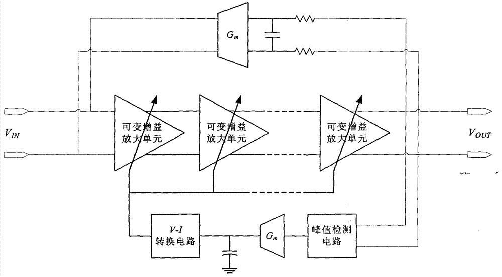
[0048] figure 1 It is a block diagram of an automatic gain control amplifier with a DC offset elimination function in the existing common technology. Its offset elimination feedback circuit is composed of transconductance unit Gm and RC filter, and the AGC feedback circuit is composed of peak detector, transconductance unit Gm, integrating capacitor and V-I conversion circuit. The automatic gain control amplifier with the DC offset elimination function in the prior art has the following defects: the DC offset elimination feedback loop DC gain is small, so the high-pass corner frequency is relatively high, and the resistance-capacitance filter is difficult to realize under the requirements of the integration level of the whole chip The low-pass frequency is small, so the closed-loop high-pass corner frequency of the entire circuit is high, and the loss of low-frequency signals is large.

[0049] The present invention proposes an automatic gain control amplifier that eliminates...


PUM


Abstract

The invention discloses a complementary metal oxide semiconductor (CMOS) automatic gain control amplifier for canceling direct current offset. The CMOS automatic gain control amplifier comprises a cascade amplification link, an automatic gain control feedback loop and a direct current offset canceling feedback loop. The cascade amplification link uses multistage variable gain amplification units for cascading and can achieve high gain and enlarge high gain dynamic ranges. The automatic gain control feedback loop uses a charge pump structure and has the advantages that the automatic gain control feedback loop is less influenced by process deviation and temperature deviation, is capable of accurately detecting narrow-band and wide-band signal amplitude and is suitable for achieving CMOS processes. The direct current offset canceling feedback loop uses two-stage negative feedback loops, and each of the two-stage negative feedback loops uses an integrator as low-pass negative feedback; an active device is used as an integrator input resistor, and an equivalent resistor is provided with characteristics of temperature compensation; and the automatic gain control amplifier for canceling the direct current offset is capable of effectively canceling the direct current offset superposed by a preceding stage circuit and the direct current offset of the amplification link and is provided with a lower high pass corner frequency and a higher integrated level, and the automatic gain control amplifier for canceling the direct current offset is small in low-frequency signal loss and requires no off-chip passive devices (high value resistors or capacitors and the like). The automatic gain control amplifier is applicable to wireless communication receivers with zero intermediate frequency structures in the CMOS processes.

Description

technical field [0001] The invention belongs to the technical field of digital communication, relates to an automatic gain control amplifier, in particular to an automatic gain control amplifier for eliminating direct current offset, which is used to realize a highly integrated automatic gain control amplifier with the function of eliminating direct current offset. Background technique [0002] For wireless receivers, due to the large change in the strength of the received signal, or the deviation of the gain of the off-chip or RF front-end circuit, the amplitude of the analog baseband signal after frequency conversion changes drastically, resulting in a serious deterioration in the performance of the analog-to-digital converter. The baseband cannot be demodulated correctly, so it is necessary to introduce an automatic gain control amplifier for adjustment, so that the signal received by the analog-to-digital converter has a stable amplitude, reducing the impact of the amplit...

Claims


Application Information

Patent Timeline
IPC IPC(8): H03G3/30
Inventor 黄伟马成炎叶甜春
Owner 杭州中科微电子有限公司
Why Eureka
Try Eureka