Stress silicon (Si) vertical-channel P-channel metal-oxide semiconductor (PMOS) device and preparation method

A vertical channel, integrated device technology, used in semiconductor/solid-state device manufacturing, semiconductor devices, electrical components, etc., can solve problems such as rising production costs, waste of resources and energy, and restricting the development of the semiconductor industry

Inactive Publication Date: 2012-12-05
XIDIAN UNIV
View PDF4 Cites 1 Cited by
  • Summary
  • Abstract
  • Description
  • Claims
  • Application Information

AI Technical Summary

Problems solved by technology

After years of accumulation, the world has invested more than one trillion US dollars in equipment and technology in the microelectronics industry. If the process technology is only improved through the replacement of equipment, a generation of equipment will be eliminated every 18 months, which will cause huge losses. The waste of resources and energy leads to an increase in production costs. Therefore, this situation seriously restricts the development of the semiconductor industry

Method used


Image

  • Stress silicon (Si) vertical-channel P-channel metal-oxide semiconductor (PMOS) device and preparation method
  • Stress silicon (Si) vertical-channel P-channel metal-oxide semiconductor (PMOS) device and preparation method
  • Stress silicon (Si) vertical-channel P-channel metal-oxide semiconductor (PMOS) device and preparation method

Examples


Embodiment 1

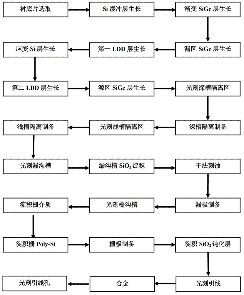
[0073] Embodiment 1: prepare the strained Si vertical channel PMOS integrated device circuit whose conductive channel is 45nm, the specific steps are as follows:

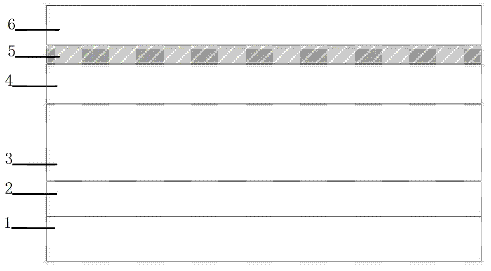
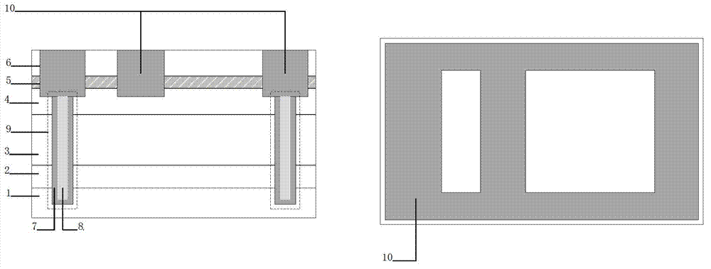
[0074] Step 1, epitaxial material preparation, as shown in Figure 2(a).

[0075] (1a) Select the doping concentration to be 5×10 15 cm -3 Left and right N-type Si substrate sheets 1;

[0076] (1b) Using chemical vapor deposition (CVD), grow a P-type Si epitaxial layer 2 with a thickness of 400 nm on the substrate at 600 °C, with a doping concentration of 5×10 15 cm -3 ;

[0077] (1c) A P-type SiGe buffer layer 3 with a thickness of 1.5 μm is grown on the Si epitaxial layer at 600°C by chemical vapor deposition (CVD), and the Ge composition gradually changes from bottom to top. 0% to 15%, the doping concentration is 5×10 18cm -3 ;

[0078] (1d) Using chemical vapor deposition (CVD), at 600°C, grow a P-type SiGe layer 4 with a thickness of 300 nm on the SiGe epitaxial layer as the drain region, with a doping c...

Embodiment 2

[0109] Embodiment 2: the preparation of the strained Si vertical channel PMOS integrated device and circuit with a conductive channel of 30nm, the specific steps are as follows:

[0110] Step 1, epitaxial material preparation, as shown in Figure 2(a).

[0111] (1a) Select the doping concentration to be 5×10 15 cm -3 Left and right N-type Si substrate sheets 1;

[0112] (1b) Using chemical vapor deposition (CVD), grow a P-type Si epitaxial layer 2 with a thickness of 200 nm on the substrate at 700 °C, with a doping concentration of 5×10 15 cm -3 ;

[0113] (1c) Using chemical vapor deposition (CVD), grow a P-type SiGe buffer layer 3 with a thickness of 1 μm on the Si epitaxial layer at 700 ° C. The Ge composition gradually changes, and the distribution is from bottom to top from 0 to 20%, the doping concentration is 7×10 18 cm -3 ;

[0114] (1d) Using chemical vapor deposition (CVD), at 700°C, grow a p-type SiGe layer 4 with a thickness of 200 nm on the SiGe layer as th...

Embodiment 3

[0145] Embodiment 3: The strained Si vertical channel PMOS integrated device and the circuit that the preparation conduction channel is 22nm, concrete steps are as follows:

[0146] Step 1, epitaxial material preparation, as shown in Figure 2(a).

[0147] (1a) Select the doping concentration to be 5×10 16 cm -3 Left and right N-type Si substrate sheets 1;

[0148] (1b) A P-type Si epitaxial layer 2 with a thickness of 300nm was grown on the substrate at 750°C by chemical vapor deposition (CVD), and the doping concentration was 5×10 16 cm -3 ;

[0149] (1c) A P-type SiGe buffer layer 3 with a thickness of 1.25 μm is grown on the Si epitaxial layer at 750°C by chemical vapor deposition (CVD). The Ge composition gradually changes from bottom to top. 0% to 25%, the doping concentration is 5×10 19 cm -3 ;

[0150] (1d) Using chemical vapor deposition (CVD), at 750°C, grow a P-type SiGe layer 4 with a thickness of 250 nm on the SiGe epitaxial layer as the drain region, with ...


PUM

PropertyMeasurementUnit
thicknessaaaaaaaaaa
thicknessaaaaaaaaaa
thicknessaaaaaaaaaa

Abstract

The invention discloses a stress silicon (Si) vertical-channel P-channel metal-oxide semiconductor (PMOS) integration device prepared by a micrometer level process and a preparation method. The method is characterized in that a PMOS device is formed through an epitaxial material preparation step, an isolator preparation step, a drain connecting region preparation step and a PMOS forming step; and finally a PMOS integration circuit with the length of a conducting channel of 22 to 45nm is formed through a step for forming the PMOS integration circuit. By utilizing the characteristic that the hole mobility of the stress Si is higher than that of relaxation Si, on the platform of a micrometer-level Si integration circuit processing technique, the stress Si vertical-channel PMOS integration device and the circuit with excellent performance are manufactured under low temperature.

Description

technical field [0001] The invention belongs to the technical field of semiconductor integrated circuits, in particular to a strained Si vertical channel PMOS integrated device and a preparation method. Background technique [0002] The new technological revolution is also called the modern technological revolution, and some people call it the third technological revolution after the steam engine and electricity. Information technology with microelectronics technology, electronic computer, laser, optical fiber communication, satellite communication and remote sensing technology as the main content has become the leading technology of the new technology revolution. The new technology revolution emerged in the mid-1940s. It first emerged in the western developed capitalist countries, and gradually radiated to other countries and regions until it swept the world. It developed along with the formation of contemporary science and technology, and has expanded to scientific variou...

Claims


Application Information

Patent Timeline
Patent Type & Authority Applications(China)
IPC IPC(8): H01L29/78H01L29/10H01L21/336
Inventor 张鹤鸣王海栋胡辉勇宋建军宣荣喜王斌周春宇郝跃
Owner XIDIAN UNIV
Why Eureka
Try Eureka