
Method for manufacturing phase change memory

A technology of phase-change memory and manufacturing method, which is applied in semiconductor/solid-state device manufacturing, electrical components, circuits, etc., can solve problems such as device leakage, yield reduction, and substrate material cannot be completely removed, and achieve simplified process and process simple effect

Active Publication Date: 2012-12-05
SEMICON MFG INT (SHANGHAI) CORP
View PDF6 Cites 8 Cited by
  • Summary
  • Abstract
  • Description
  • Claims
  • Application Information

AI Technical Summary

Problems solved by technology

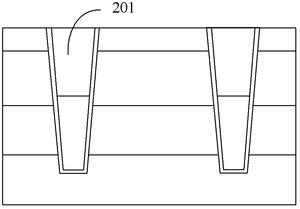
[0006] However, ideally, the sidewalls of the deep trenches are perpendicular to the substrate surface. However, in the actual process, the deep trenches formed by etching have an inverted trapezoidal shape, and the polysilicon and silicon dioxide filled in the deep trenches also form an inverted trapezoidal shape. outline (such as image 3 shown), when the substrate is subsequently dry-etched to form a shallow trench isolation region, the substrate material on both sides of the deep trench isolation region with the same depth as the shallow trench isolation region cannot be completely removed, Thus forming wedge-shaped residues on both sides of the deep trench isolation region (such as Figure 4 Mark 205 position in ) wedge-shaped residues are easy to form a conductive path between different memory cells, so that the device leaks electricity and the yield rate is correspondingly reduced

Method used


Image

  • Method for manufacturing phase change memory
  • Method for manufacturing phase change memory
  • Method for manufacturing phase change memory

Examples


Embodiment Construction

[0032] In the following description, many specific details are explained in order to fully understand the present invention. However, the present invention can be implemented in many other ways different from those described here, and those skilled in the art can make similar popularizations without violating the connotation of the present invention. Therefore, the present invention is not limited by the specific implementation disclosed below.

[0033] Secondly, the present invention is described in detail by using schematic diagrams. When describing the embodiments of the present invention in detail, the schematic diagrams are merely examples, which should not limit the scope of protection of the present invention.

[0034] reference Figure 7 , Shows a schematic flow chart of an embodiment of a method for manufacturing a phase change memory of the present invention, and the method roughly includes the following steps:

[0035] Step S1, providing a semiconductor substrate, which in...


PUM


Abstract

A method for manufacturing a phase change memory comprises the steps of providing a semiconductor substrate; imaging a first hard mask layer to form a first hard mask image; etching the first hard mask image used as a mask so as to form deep grooves; forming a liner layer for covering the deep grooves without damaging the shapes of the deep grooves; filling a semiconductor material in the deep grooves coated with the liner layer to form a semiconductor layer; removing a part of the liner layer positioned on the semiconductor layer; depositing a dielectric material on the semiconductor layer until the deep grooves are filled with the dielectric material; removing the redundant dielectric material through a planarization process until a second hard mask layer is exposed; imaging the second hard mask layer to form a second hard mask image; removing a part of the exposed dielectric layer of the second hard mask image by ashing, and forming a recess encircled by the rest dielectric layer and an epitaxial layer; and moving a part of the epitaxial layer by using the second hard mask image as a mask so as to form shallow grooves. The method for manufacturing the phase change memory is simple.

Description

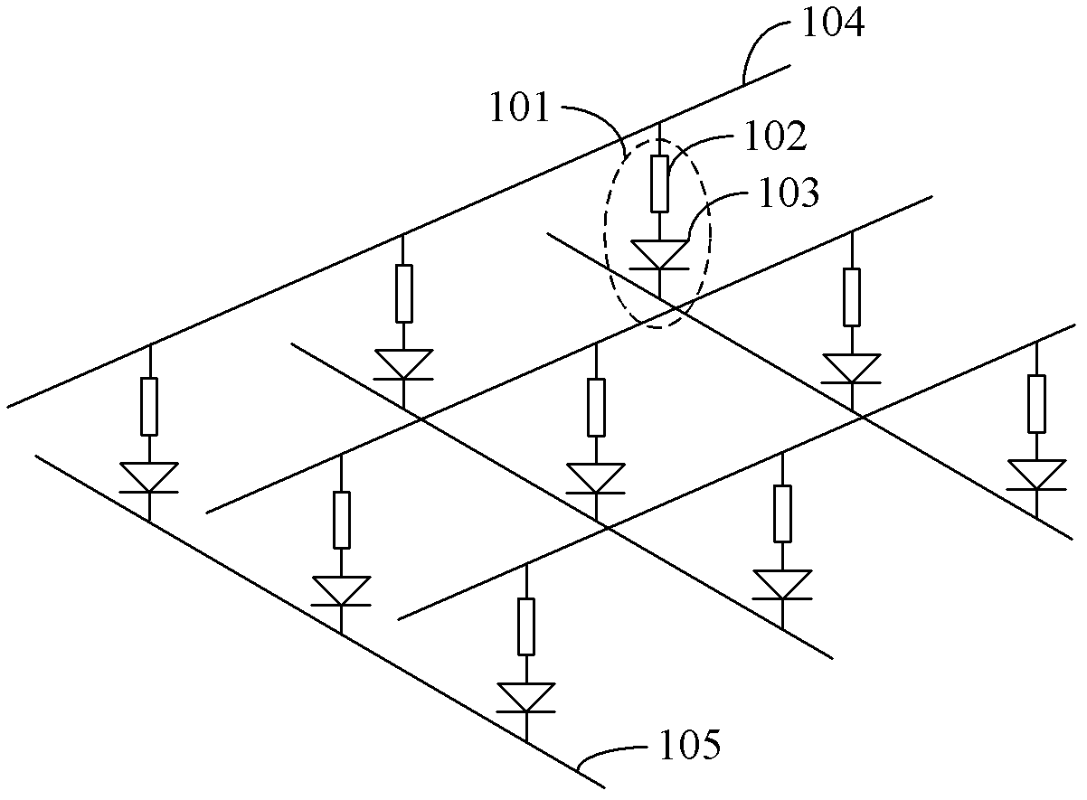
Technical field [0001] The present invention relates to the field of semiconductor technology, and more specifically, the present invention relates to a method for manufacturing a phase change memory. Background technique [0002] Phase Change Random Access Memory (PCRAM), as an emerging non-volatile storage technology, is used for flash memory in terms of read and write speed, read and write times, data retention time, cell area, and multi-value realization. Both have great advantages. [0003] US Patent US6531373 discloses a phase change memory structure, such as figure 1 As shown, each memory cell 101 of the phase change memory includes a phase change resistor 102 and a strobe diode 103 connected in series. When the phase change memory is written, a large potential difference is formed between the bit line 104 and the word line 105 corresponding to a certain memory cell 101 to be selected, and the potential difference makes the gate diode 103 forward conduction, In turn, a rel...

Claims


Application Information

Patent Timeline
Patent Type & Authority Applications(China)
IPC IPC(8): H01L45/00H01L21/762
Inventor HE QIYANGZHANG YIYING
Owner SEMICON MFG INT (SHANGHAI) CORP
Learn More