Structure for improving performance of passive device of power integrated circuit

A passive device and integrated circuit technology, applied in the field of microelectronics, can solve the problems of lower reliability, higher cost, high doping concentration of the substrate, etc., and achieve the effect of reducing area, reducing loss and increasing thickness

Inactive Publication Date: 2012-12-12
KUNSHAN HUATAI ELECTRONICS TECH CO LTD
View PDF12 Cites 1 Cited by
  • Summary
  • Abstract
  • Description
  • Claims
  • Application Information

AI Technical Summary

Problems solved by technology

However, power integrated circuits usually have a high doping concentration on the substrate, and directly making passive devices such as inductors or capacitors on it will bring very large losses.
Therefore, current high-power amplifiers are usually based on discrete power devices, and a large number of passive devices such as inductors or capacitors are required outside the chip to achieve a high quality factor, which greatly increases costs and reduces reliability.

Method used


Image

  • Structure for improving performance of passive device of power integrated circuit
  • Structure for improving performance of passive device of power integrated circuit
  • Structure for improving performance of passive device of power integrated circuit

Examples


Embodiment 1

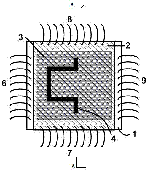
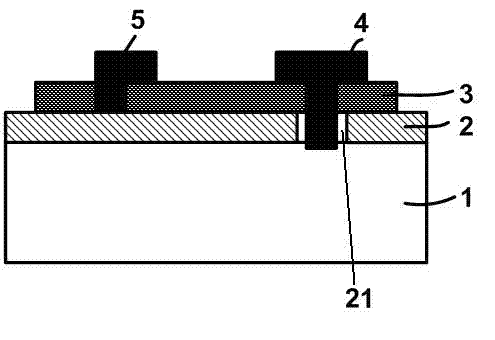
[0026] Such as figure 1 with figure 2 As shown, the power integrated circuit chip includes a substrate 1, a metal plate 2, an insulating layer 3 and a closed pin 6 of the chip, and the package is in the form of a bonding wire. The substrate 1 is used to form power devices and some of the most basic passive devices, which do not require very high quality factors, such as bias resistors and DC decoupling capacitors. It contains several layers of metal, which are used for wiring. The metal plate 2 is to improve isolation between passive devices and active devices. The metal plate 2 is usually grounded, and the source terminal of the power device is also connected to the metal plate 2 to form a current loop. The insulating layer 3 needs to have a certain thickness, usually greater than 60 μm. The thick metal on the metal plate 2 can be used as a passive device to improve the quality factor of the passive device, and the thickness is usually greater than 10 . 4 and 5 show t...

Embodiment 2

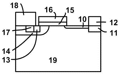
[0029] In this embodiment, the present invention is described in conjunction with the structure of the power device LDMOS in the power integrated circuit, and the structure of the N-type LDMOS is taken as an example for illustration, and the same principle is used for the P-type LDMOS and the N-type LDMOS.

[0030] Such as image 3 As shown, the power device LDMOS includes a gate 16 , a source 13 and a drain 11 . The source terminal 13 of this power integrated circuit is not grounded through the substrate 19, but is grounded through a large metal plate in the power integrated circuit. Therefore, compared with the traditional power integrated circuit, the resistivity of the substrate can be increased, which can reduce the loss. . The source 13 and the drain 11 are heavily doped N-type sources and drains, and the doping concentration is usually 10 19 / cm 3 As above, the metal interconnections 18 and 12 are respectively connected to the source 13 and the drain 11 . The source...

Embodiment 3

[0032] In this embodiment, on the basis of Embodiment 1, further improvements are made. Such as Figure 4 As shown, the substrate 1 is pierced by the TSV (Through-Silicon-Via) method, and a through channel 20 is formed on the substrate 1, and the metal plate 2 is connected to the backside of the substrate through the channel 20. The heat sink dissipates heat. In this way, the substrate 1 can be attached to the conductive heat sink, and the grounding is naturally realized without using Bondwire or flip-chip welding to lead out the source. These two methods can also be used at the same time, which can further reduce the parasitic inductance and resistance, and improve the efficiency of the device. All the other are identical with embodiment 1.


PUM


Abstract

The invention discloses a structure for improving the performance of a passive device of a power integrated circuit. A metal plate is arranged in a chip of the power integrated circuit. The passive device is separated from an active device, the passive device is piled on a substrate and an area of the integrated circuit is reduced. One layer serving as the passive device is free from complex wiring, therefore, the thickness of a metal can be increased and the loss of the device can be reduced. A large metal plate can separate an electric field, and the passive and active devices do not affect each other. No electromagnetic field enters the substrate which is usually damaged, therefore, the energy loss can be reduced, and the performance of the passive device can be improved. The thickness of the chip is increased by pile-up on a power chip, so that the thickness of a silicon wafer can be reduced, and the silicon wafer is not bended, a radiating capacity of the chip is greatly improved. A source end is directly connected with the large metal plate, and the substrate is not used as a conductive layer, so that doping concentration of the substrate is reduced, and performances of the passive and active devices are improved.

Description

technical field [0001] The invention relates to a structure for improving the performance of a power integrated circuit passive device, which belongs to the field of microelectronic technology. Background technique [0002] The radio frequency and microwave fields require a large number of power amplifiers to obtain high output power to increase the transmission distance. At the same time, the power amplifiers are required to have high efficiency to reduce the cost of heat dissipation. Silicon-based LDMOS is widely used in radio frequency and microwave fields to realize power amplifiers because of its high power gain and high breakdown voltage. [0003] Power integrated circuits not only need active power devices, but also passive devices for input, output and inter-stage impedance matching. However, the doping concentration of the substrate of power integrated circuits is usually very high, and directly making passive devices such as inductors or capacitors on it will brin...

Claims


Application Information

Patent Timeline
Patent Type & Authority Applications(China)
IPC IPC(8): H01L23/552H01L23/50H01L23/367
CPCH01L2924/0002H01L2924/00
Inventor 曾大杰余庭赵一兵张耀辉
Owner KUNSHAN HUATAI ELECTRONICS TECH CO LTD
Why Eureka
Try Eureka