Tunneling field effect transistor

A tunneling field effect, transistor technology, applied in the direction of transistors, semiconductor devices, electrical components, etc., can solve the problems of small sub-threshold slope, small on-state current, etc., achieve low sub-threshold slope, low off-state current, improve open The effect of state current

Inactive Publication Date: 2012-12-19
PEKING UNIV
View PDF4 Cites 15 Cited by
  • Summary
  • Abstract
  • Description
  • Claims
  • Application Information

AI Technical Summary

Problems solved by technology

Tunneling field effect transistors have the advantages of small leakage current and small subthreshold slope, but because they use the tunneling effect to generate current, their on-state current is smaller than that of metal insulating layer field effect transistors.

Method used


Image

  • Tunneling field effect transistor
  • Tunneling field effect transistor
  • Tunneling field effect transistor

Examples


Embodiment 1

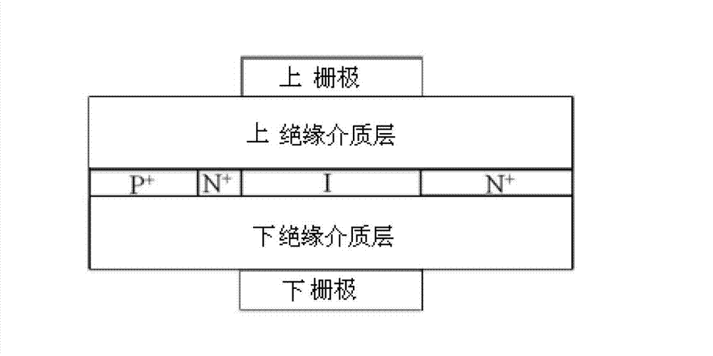
[0036] Such as figure 1 As shown, this embodiment provides a tunneling field effect transistor, including a source region, a channel region and a drain region, the source region and the drain region are respectively formed on both sides of the channel region, and the source region and the drain region The contact region of the channel region is made of extrinsic material, and the channel region is made of intrinsic material, and the doping type is different from that of the source region.

[0037] In this embodiment, the source region adopts P-type doping, the contact region between the source region and the channel region adopts N-type doping, the drain region adopts N-type doping, and the channel region adopts two-dimensional materials, such as graphene, Molybdenum disulfide (MoS2), silicene (Silicene), germanene (Germanene), boron nitride (BN), etc., preferably graphene.

[0038] In this embodiment, the tunneling field effect transistor further includes an upper insulating...

Embodiment 2

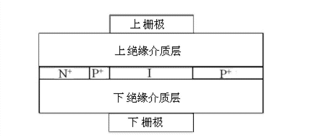
[0043] The structure of this embodiment is as figure 2 As shown, the difference between this embodiment and the first embodiment lies in that the doping method is different, so that it uses different carriers for transport. Specifically, in this embodiment, the source region is doped with N type, so The contact area between the source region and the channel region adopts P-type doping, and the drain region adopts P-type doping.

[0044] It can be seen that, compared with the structure of the N-I-P junction used in the traditional tunneling field effect transistor, in this embodiment, the part of the source close to the channel is doped with electrons, that is, P-type doping, and finally an N-P-I-P junction is formed, thereby forming NPIP type tunneling field effect transistor.

Embodiment 3

[0046] The structure of this embodiment is as Figure 4 As shown, the difference between this embodiment and the first embodiment is that the two-layer structure composed of the lower gate and the lower insulating dielectric layer in the first embodiment is replaced by a substrate.

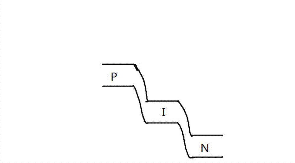
[0047] It can be seen from the above examples that since the doping at the contact between the source region and the channel region can form a structure similar to a PN junction in this part, the energy in the doped (for example N-type) region will move to the low energy direction , and then the conduction band bottom of the doped (for example N-type) region will be lower than the conduction band bottom of the channel. Figure 3a and Figure 3b shown), therefore, the present invention makes the device have a narrower tunneling layer thickness from the source end to the channel when the device is in the on state, thereby improving on-state current. Since the method does not change the thickness ...


PUM


Abstract

The invention relates to the technical field of field effect transistors and discloses a tunneling field effect transistor. The tunneling field effect transistor comprises a source region, a channel region and a drain region, wherein the source region and the drain region are respectively formed on the two sides of the channel region, and a contact region between the source region and the channel region is made of extrinsic materials and different from the doping type of the source region. According to the invention, the contact area between the source region and the channel region is doped differently from the source region, so that the device is relatively narrow in a tunneling layer from the source end to the channel in an ON state, and the ON-state current is increased. As the thickness of a tunneling layer from the source end to the drain end in an OFF state is not changed with the method, a relatively low OFF-state current can be kept, as a result, a higher switch ratio and a relatively low sub-threshold slope can be acquired with the method, so that a better device performance can be acquired.

Description

technical field [0001] The invention relates to the technical field of field effect transistors, in particular to a tunneling field effect transistor. Background technique [0002] Tunneling field-effect transistors have attracted extensive attention due to their advantages such as low power consumption and low subthreshold slope. Tunneling field effect transistors are different from traditional field effect transistors, and use tunneling effect to transport charges. Tunneling field effect transistors can work at lower driving voltages, and at the same time, the subthreshold slope is lower than the limit of 60meV / decade[1][2] of traditional field effect transistors. Recently, carbon-based materials have been used as channel materials for tunneling field-effect transistors due to their unique properties. Theoretical studies have found that the subthreshold slope of tunneling field effect transistors composed of carbon nanotubes and graphene nanoribbons can be lower than 60m...

Claims


Application Information

Patent Timeline
Patent Type & Authority Applications(China)
IPC IPC(8): H01L29/788H01L29/08
Inventor 刘飞刘晓彦康晋锋杜刚王漪
Owner PEKING UNIV
Why Eureka
Try Eureka