
Two-operation-mode ultraviolet detector with vertical structure and preparation method thereof

A dual-mode, UV detector technology, used in semiconductor devices, final product manufacturing, sustainable manufacturing/processing, etc., can solve the problems of slow device response, no gain, non-linearity, etc., and achieve high operating reliability. , without etching, the effect of simple preparation process

Active Publication Date: 2015-04-08
CHINA INFORMATION & ELECTRONICSE DEV HEFEI
View PDF3 Cites 0 Cited by
  • Summary
  • Abstract
  • Description
  • Claims
  • Application Information

AI Technical Summary

Problems solved by technology

Among the above structures, photoconductive detectors are attractive because they have high responsivity and are easy to manufacture, and are suitable for low-cost ultraviolet light monitoring (such as flame sensing), but such devices usually have high Dark current, and high photoconductive gain often severely limit the bandwidth of the device, making the device respond slowly, the response is nonlinear, and it has obvious response to sub-bandgap light
Schottky barrier and p-i-n structure have the characteristics of low dark current and high response speed, which are suitable for high-speed ultraviolet detection. However, these two structural devices have no gain in theory, and are not as good as photoconductive devices in detecting weak optical signals.

Method used


Image

  • Two-operation-mode ultraviolet detector with vertical structure and preparation method thereof
  • Two-operation-mode ultraviolet detector with vertical structure and preparation method thereof
  • Two-operation-mode ultraviolet detector with vertical structure and preparation method thereof

Examples


preparation example Construction

[0041] The preparation method of the above-mentioned vertical structure dual working mode ultraviolet photodetector selected by the bias voltage includes the following steps:

[0042] 1) Epitaxially grow wide bandgap semiconductor thin film materials on homogeneous or heterogeneous substrates, which can be single-layer films or multilayer films. The basic feature is that the uppermost film has a band gap greater than 3.1eV and has High resistance characteristics, its resistivity value> 10 6 Ω·cm, the thickness of the uppermost film is between 50nm and 1mm; wide-gap semiconductor materials include ternary or quaternary alloy materials of GaN, AlN, ZnO, MgO, GaN, AlN, ZnO and MgO. SiC, Diamond, TiO 2 Wait.

[0043] 2) Use semiconductor micromachining technology to make ohmic contact electrodes on the back of the substrate; make Schottky contact electrodes on the semiconductor active layer. Schottky electrodes can take many forms, such as ring, square, and interdigital, etc. .

[0044...


PUM


Abstract

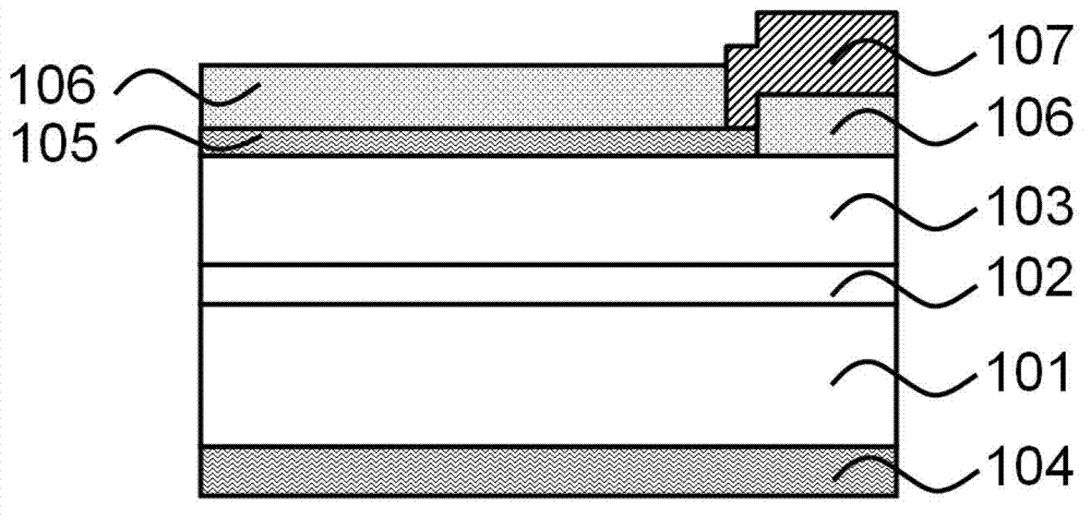
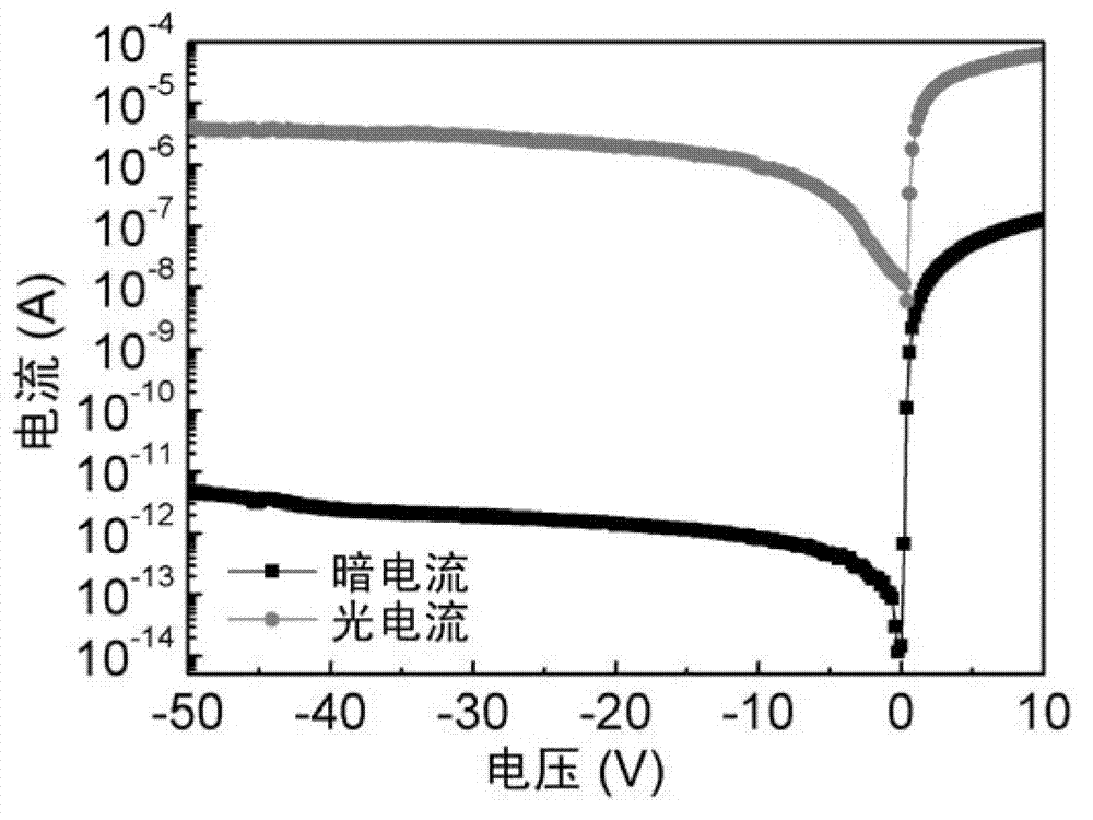
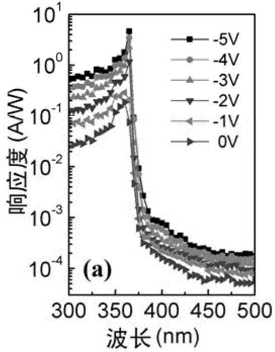
The invention discloses a two-operation-mode ultraviolet detector with a vertical structure and a preparation method of the two-operation-mode ultraviolet detector with the vertical structure. The detector of the invention comprises a substrate, a buffer layer, an ohmic electrode, a wide bandgap semiconductor light absorption layer, a schottky electrode, an insulating medium passivation layer and a contact electrode, wherein when the detector is in an operation state, and reverse bias voltages or no bias voltage is applied to the contact electrode and the ohmic electrode, the detector operates in a depletion mode; and when forward bias voltages are applied to the contact electrode and the ohmic electrode, the operation mode of the detector is converted from a schottky barrier depletion mode to a photoconduction mode, and the detector shows higher gains, specifically a gain factor is greater than 10. The two-operation-mode ultraviolet detector with the vertical structure has the advantages of high reliability, simple manufacturing process, no need for etching and the like.

Description

Technical field [0001] The invention belongs to the technical field of semiconductor optoelectronic devices, and relates to a vertical structure dual working mode ultraviolet detector and a preparation method thereof, in particular to a dual working mode ultraviolet detector selected by a vertical structure bias voltage and a preparation method thereof. Background technique [0002] Ultraviolet detection technology is another dual-use photoelectric detection technology developed after infrared and laser detection technology. Military field: The most direct application of ultraviolet detection technology is missile early warning and tracking. Ultraviolet detectors detect targets by detecting ultraviolet radiation in missile plume and provide early warning for ground weapons and equipment. Civilian field: In medicine and biology, especially in the diagnosis of skin diseases in recent years, ultraviolet detection technology has a unique application effect. UV detection technology c...

Claims


Application Information

Patent Timeline
Patent Type & Authority Patents(China)
IPC IPC(8): H01L31/108H01L31/18
CPCY02P70/50
Inventor 谢峰陆海王国胜郭进
Owner CHINA INFORMATION & ELECTRONICSE DEV HEFEI
Learn More