Fully-integrated photoelectric conversion receiver based on standard CMOS (complementary metal-oxide-semiconductor transistor) process

A photoelectric conversion and receiver technology, applied in the field of communications, can solve the problems of slow decline of the optical frequency response curve, small channel attenuation, limited performance of the photoelectric receiver, etc., to achieve the effect of improving Jitter and bit error rate

Inactive Publication Date: 2012-12-19
PEKING UNIV
View PDF2 Cites 13 Cited by
  • Summary
  • Abstract
  • Description
  • Claims
  • Application Information

AI Technical Summary

Problems solved by technology

[0003] Because the optical interconnection between chips has the following advantages: no interface reflection, small channel attenuation, no binding inductance, no interface ESD, and easy multi-chip integration, but the current technology development also has the following unresolved problems: At present, silicon-based standard CMOS photodetectors cannot meet the two requirements of high intrinsic bandwidth and high responsivity required for high-speed optical communication at the same time. It is difficult to realize high-modulation optical transmitters through standard processes, and the transmission medium needs to be changed, etc.
[0005] Silicon-based standard CMOS process to achieve monolithic integration of optical receivers also faces some challenges and problems: the responsivity of photodetectors based on standard CMOS processes is insufficient, an

Method used


Image

  • Fully-integrated photoelectric conversion receiver based on standard CMOS (complementary metal-oxide-semiconductor transistor) process
  • Fully-integrated photoelectric conversion receiver based on standard CMOS (complementary metal-oxide-semiconductor transistor) process
  • Fully-integrated photoelectric conversion receiver based on standard CMOS (complementary metal-oxide-semiconductor transistor) process

Examples


Example Embodiment

[0031] The present invention will be further described below in conjunction with the embodiments in the accompanying drawings:

[0032] First introduce the main circuit modules:

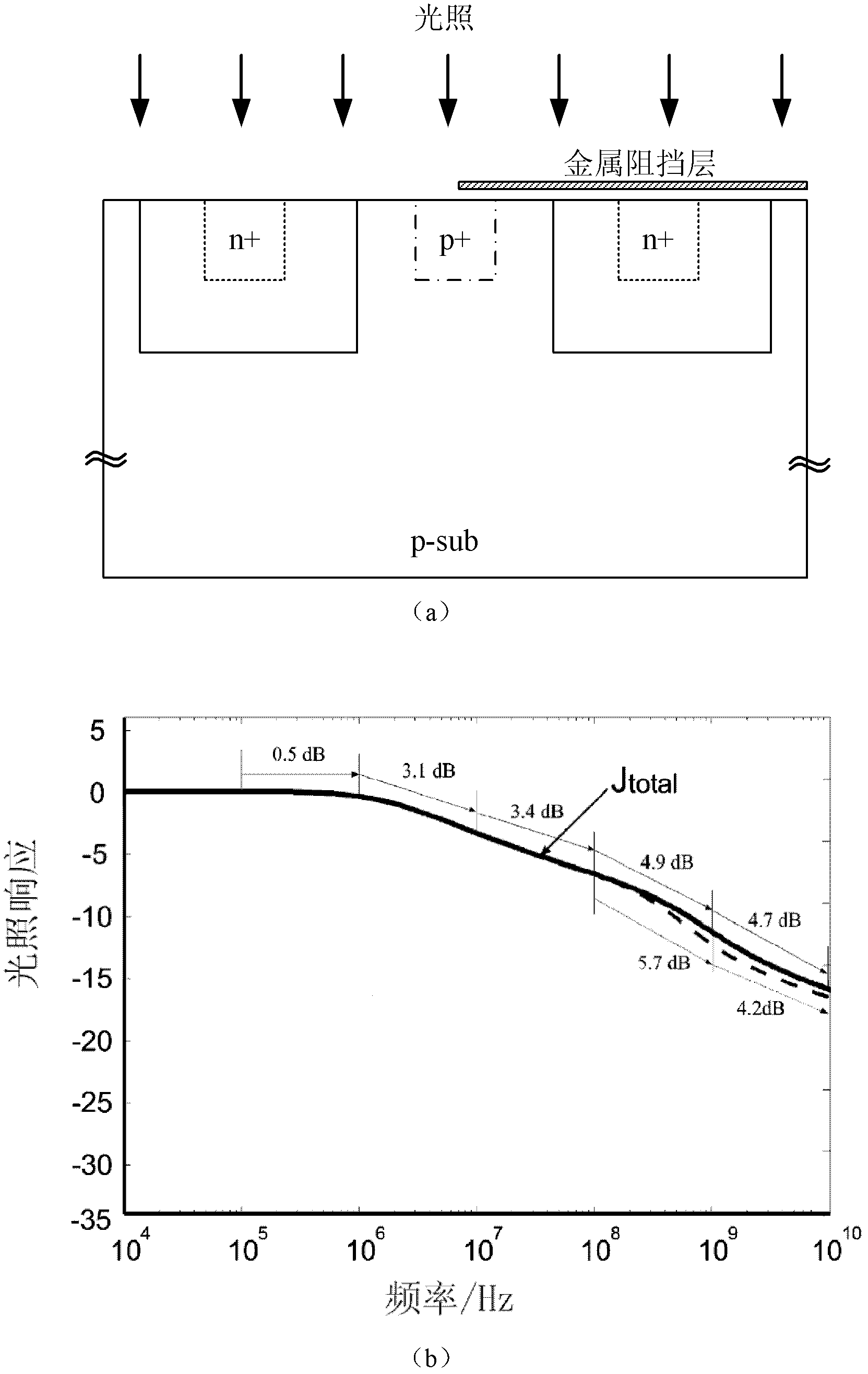
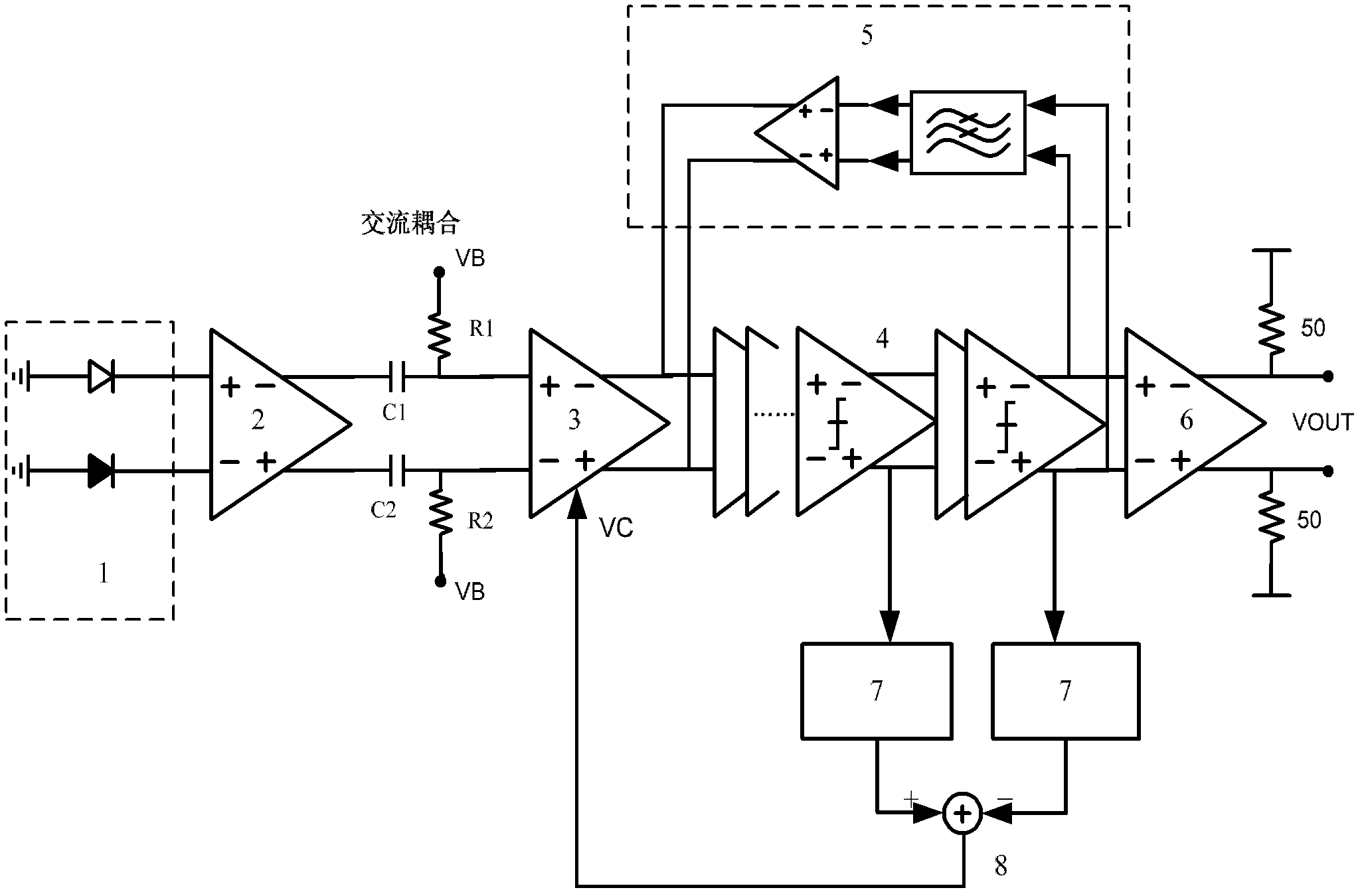
[0033] PD: Photodetector ( figure 2 module in 1)

[0034] TIA: Transconductance amplifier, mainly realizes the conversion of current to voltage ( figure 2 in module 2)

[0035] Equalizer: Equalizer to compensate for the high frequency components of the signal ( figure 2 in module 3)

[0036] LA: Limiter, amplifies the signal ( figure 2 in module 4)

[0037] DCOC: DC Skew Cancellation Module ( figure 2 in module 5)

[0038] OutputBuffer: output buffer ( figure 2 in module 6)

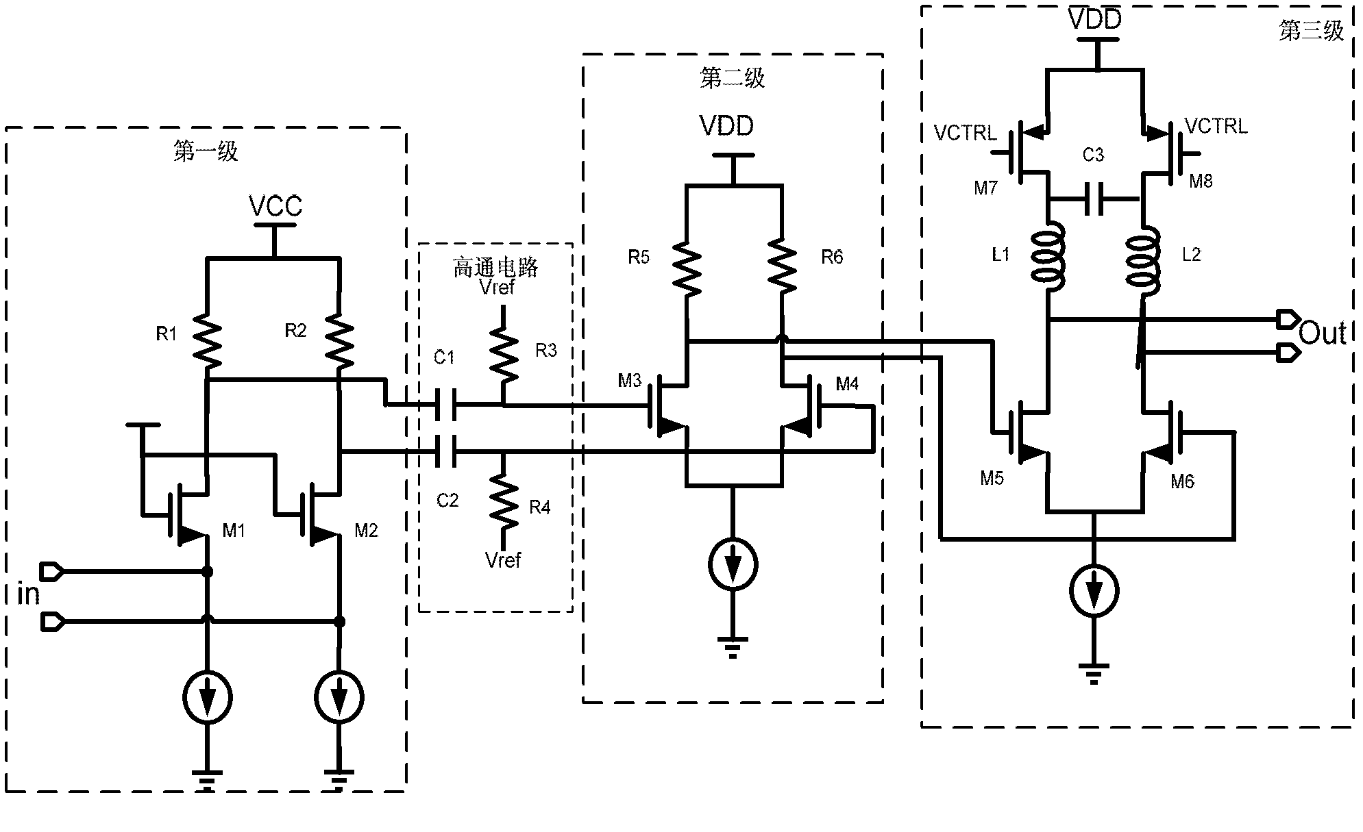
[0039] Slope Detector: A slope detector that converts an AC signal to a DC signal ( figure 2 module 7) in the Figure 4 The circuit structure shown is implemented, the input signal is first passed through a high-pass filter, and then a shaper (Rectifier) ​​is performed to obtain a feedback control component cont...


PUM


Abstract

The invention relates to a fully-integrated photoelectric conversion receiver based on standard CMOS process. The fully-integrated photoelectric conversion receiver comprises a photoelectric detector, a trans-conductance amplifier, an equalizer, a multi-stage limiter, a DCOC (decentralized classic optimal control) processing circuit, an output buffer, a slope detector and an error amplifier, wherein the P end of the photoelectric detector is grounded, and the N end is connected with the input end of the trans-conductance amplifier; the trans-conductance amplifier is connected with the differential input end of the equalizer through a high-pass circuit; the output end of the equalizer is connected with the differential input end of the output buffer through the multi-stage limiter; and the differential input end of the input buffer is connected with the output end of the equalizer through the DCOC processing circuit. The fully-integrated photoelectric conversion receiver provided by the invention is adaptive to transmission with higher data rate, can suppress jitter and error rate, can realize self-adaptive regulation, and can be widely used in the field of communication technology.

Description

Technical field [0001] The invention belongs to the technical field of communication, and relates to a photoelectric conversion receiver, in particular to a fully integrated photoelectric conversion receiver based on a standard CMOS process. Background technique [0002] Nowadays, with the continuous improvement of the speed of various communication protocols, 10Gb / s will become the mainstream trend of wired interconnection development. Recently, some key circuit modules for 40Gb / s rate have also begun to emerge, while for single channel at least 100Gb / s or more It is an inevitable trend of development. However, with the continuous improvement of the speed, the development of the electrical interconnection itself is also limited by the channel transmission (high-frequency attenuation and interface reflection), which makes it difficult. At this time, the optical interconnection between chips is more attractive, and it is also an inevitable trend of development. [0003] Bec...

Claims


Application Information

Patent Timeline
IPC IPC(8): H04B10/06H01L27/144
Inventor 廖怀林侯中原沈灵叶乐张兴
Owner PEKING UNIV
Why Eureka
Try Eureka