Silicon-on-insulator silicon germanium heterojunction bipolar transistor (SOI SiGe HBT) planar integrated device and preparation method thereof

An integrated device and planar technology, applied in semiconductor/solid-state device manufacturing, semiconductor devices, electrical components, etc., can solve problems such as poor heat dissipation performance, low mechanical strength, and high cost

Active Publication Date: 2015-07-22
陕西半导体先导技术中心有限公司
View PDF0 Cites 0 Cited by
  • Summary
  • Abstract
  • Description
  • Claims
  • Application Information

AI Technical Summary

Problems solved by technology

Although GaAs and InP-based compound devices have superior frequency characteristics, their preparation process is more complicated than Si process, high cost, difficult to prepare large-diameter single crystal, low mechanical strength, poor heat dissipation performance, incompatibility with Si process and lack of SiO 2 Such passivation layer and other factors limit its wide application and development.

Method used


Image

  • Silicon-on-insulator silicon germanium heterojunction bipolar transistor (SOI SiGe HBT) planar integrated device and preparation method thereof

Examples


Embodiment 1

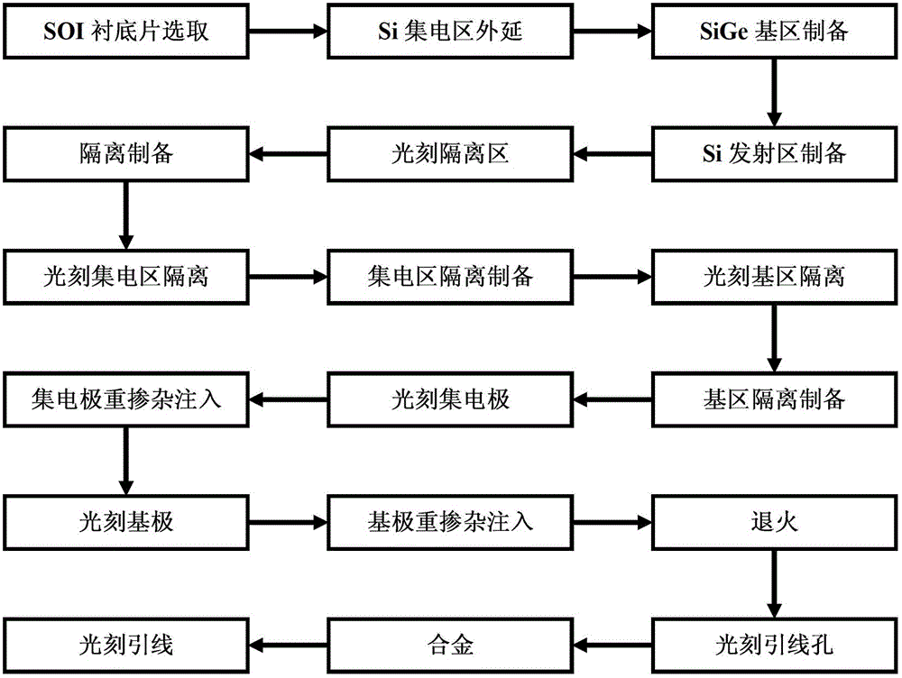
[0074] Embodiment 1: prepare the SOI SiGe HBT planar integrated device and circuit method with a base thickness of 20nm, the specific steps are as follows:

[0075] Step 1, epitaxial material preparation.

[0076] (1a) Select an SOI substrate, the support material 1 of the lower layer of the substrate is Si, and the middle layer 2 is SiO 2 , the thickness is 150nm, and the upper layer material 3 has a doping concentration of 1×10 16 cm -3 N-type Si with a thickness of 100nm;

[0077] (1b) Using chemical vapor deposition (CVD), grow a layer of N-type epitaxial Si layer with a thickness of 50nm on the upper Si material at 600°C, as the collector region, and the doping concentration of this layer is 1× 10 16 cm -3 ;

[0078] (1c) Using chemical vapor deposition (CVD), grow a layer of SiGe layer with a thickness of 20nm on the substrate at 600°C. As the base region, the Ge composition of this layer is 15%, and the doping concentration is 5×10 18 cm -3 ;

[0079] (1d) Usi...

Embodiment 2

[0109] Embodiment 2: prepare the SOI SiGe HBT planar integrated device and circuit method with a base thickness of 40nm, the specific steps are as follows:

[0110] Step 1, epitaxial material preparation.

[0111] (1a) Select an SOI substrate, the support material 1 of the lower layer of the substrate is Si, and the middle layer 2 is SiO 2 , the thickness is 300nm, and the upper material 3 has a doping concentration of 5×10 16 cm -3 N-type Si with a thickness of 120nm;

[0112] (1b) Using the method of chemical vapor deposition (CVD), grow an N-type epitaxial Si layer 4 with a thickness of 80nm on the upper Si material at 700°C as the collector region, and the doping concentration of this layer is 5 ×10 16 cm -3 ;

[0113] (1c) Using chemical vapor deposition (CVD), at 700°C, grow a layer of SiGe layer 5 with a thickness of 40nm on the substrate, as the base region, the Ge composition of this layer is 20%, and the doping concentration is 1×10 19 cm -3 ;

[0114] (1d)...

Embodiment 3

[0144] Embodiment 3: preparation of SOI SiGe HBT planar integrated device and circuit method with a base thickness of 60nm, the specific steps are as follows:

[0145] Step 1, epitaxial material preparation.

[0146] (1a) Select an SOI substrate, the support material 1 of the lower layer of the substrate is Si, and the middle layer 2 is SiO 2 , the thickness is 400nm, and the upper layer material 3 has a doping concentration of 1×10 17 cm -3 N-type Si with a thickness of 150nm;

[0147] (1b) Using the method of chemical vapor deposition (CVD), grow a layer of N-type epitaxial Si layer 4 with a thickness of 100 nm on the upper Si material at 750 ° C, as the collector region, and the doping concentration of this layer is 1 ×10 17 cm -3 ;

[0148] (1c) Using the chemical vapor deposition (CVD) method, at 750°C, grow a layer of SiGe layer 5 with a thickness of 60nm on the substrate. As the base region, the Ge composition of this layer is 25%, and the doping concentration is ...


PUM

PropertyMeasurementUnit
thicknessaaaaaaaaaa
thicknessaaaaaaaaaa
thicknessaaaaaaaaaa

Abstract

The invention discloses a silicon-on-insulator silicon germanium heterojunction bipolar transistor (SOI SiGe HBT0 planar integrated device and a preparation method thereof. The preparation method comprises following steps of continuously growing N-channel silicon (N-Si), P-channel silicon germanium (P-SiGe) and an N-channel silicon (N-Si) layer to deposit a dielectric layer to prepare shallow-trench isolation, photo-etching a collector region shallow-trench isolation area, preparing a collector region shallow-trench isolation, etching and depositing a dielectric layer, photo-etching a base-region shallow-trench isolation area, preparing a base-region shallow-trench isolation, photo-etching a collector region and injecting phosphorous ions to form a collector electrode contact region, photo-etching a base region and injecting boron ions to form a base electrode contact area, finally forming a SiGe HBT device, finally photo-etching a transmitting region lead hole, a base region lead holeand a collector region lead hole, metalizing, photo-etching leads, and forming an HBT integrated circuit with the thickness of the base region of 20 to 60nm. The technical method provided by the invention is compatible with the processing technique of the traditional CMOS integrated circuit, so that under the situation that the fund and the equipment investment are small, the SOI-based bipolar complementary metal-oxide semiconductor (BiCMOS) device and an integrated circuit are prepared, and the performance of the traditional analog and digital mixed integrated circuit is greatly improved.

Description

technical field [0001] The invention belongs to the technical field of semiconductor integrated circuits, and in particular relates to an SOI SiGe HBT planar integrated device and a preparation method. Background technique [0002] Integrated circuits are the cornerstone and core of the economic development of an information society. Just as the American engineering and technology circle recently named the fifth electronic technology among the 20 greatest engineering and technological achievements in the world in the 20th century, "from vacuum tubes to semiconductors and integrated circuits, they have become the cornerstone of intelligent work in various industries today." Integrated circuits. It is one of the typical products that can best reflect the characteristics of knowledge economy. At present, the electronic information industry based on integrated circuits has become the world's largest industry. With the development of integrated circuit technology, the clear bou...

Claims


Application Information

Patent Timeline
Patent Type & Authority Patents(China)
IPC IPC(8): H01L29/08H01L29/737H01L21/331
Inventor 宋建军胡辉勇吕懿张鹤鸣宣荣喜王斌舒斌郝跃
Owner 陕西半导体先导技术中心有限公司
Why Eureka
Try Eureka