Method for preparing low-stress GaN film

A low-stress, thin-film technology, applied in semiconductor/solid-state device manufacturing, electrical components, circuits, etc., can solve the problem of performance degradation of GaN-based materials

Inactive Publication Date: 2013-01-02
NANJING UNIV
View PDF2 Cites 8 Cited by
  • Summary
  • Abstract
  • Description
  • Claims
  • Application Information

AI Technical Summary

Problems solved by technology

The presence of stress will cause the performance of GaN-based materials to decr...

Method used


Image

  • Method for preparing low-stress GaN film
  • Method for preparing low-stress GaN film
  • Method for preparing low-stress GaN film

Examples


Embodiment Construction

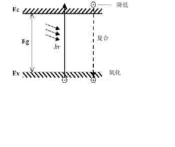
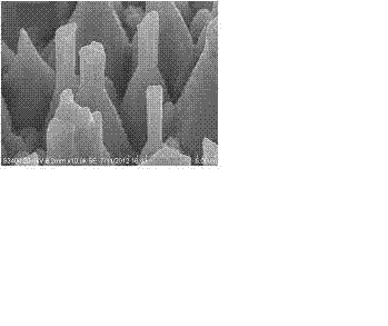
[0019] The method and process of the present invention include several parts: GaN nanostructure obtained by light-assisted electrodeless corrosion of GaN / sapphire composite substrate (referring to GaN grown on sapphire substrate); HVPE regrowth of low-stress GaN thin film.

[0020] Furthermore, the distribution and scale of the nanostructured GaN pillars can be controlled through the selection of etching time and solvent concentration (the more intense the corrosion and the longer the etching time, the thinner the size distribution and the smaller the size of the GaN pillars). In HVPE lateral epitaxy, self-separation between GaN film and sapphire can also be achieved, thereby obtaining a low-stress self-supporting GaN substrate material.

[0021] One of the technical implementations of the present invention is to prepare a low-stress GaN thin film, including the following steps:

[0022] 1. Cleaning and processing of GaN / sapphire composite substrate. The samples were ultrason...


PUM


Abstract

The invention relates to a method for preparing a low-stress GaN film. A GaN/sapphire composite substrate is corroded with a photo-assisted corrosion solvent so as to form the GaN/sapphire composite substrate in a nano-structure; the photo-assisted corrosion is the ultraviolet-assisted corrosion, the corrosion solvent is the mixed solution of strong base and oxidant, namely, the mixture in a molar concentration of 0.05-0.15 M consisting of NaOH or KOH in a molar concentration of 0.5-1.5 M and K2S2O8, and the reaction is carried out at a room temperature or a temperature below 50 DEG C for 0.5-10 hours; and the GaN/sapphire composite substrate in the nano-structure can be obtained. The method is used for reducing the stress in the GaN film material of the semiconductor material grown with the HVPE (hydride vapor phase epitaxy).

Description

technical field [0001] The invention relates to a method for electrodeless light-assisted corrosion of GaN materials and obtaining nanostructures, a method and process for reducing stress in GaN film materials grown by hydride vapor phase epitaxy (HVPE) and obtaining self-supporting GaN substrates. Background technique [0002] Group III-V nitride materials (also known as GaN-based materials) mainly composed of GaN, InGaN, and AlGaN alloy materials are new semiconductor materials that have attracted much attention in the world in recent years. GaN-based materials are direct bandgap wide bandgap semiconductor materials with continuously variable direct bandgap between 1.9-6.2eV, excellent physical and chemical stability, high saturation electron drift velocity, high breakdown field strength and high thermal conductivity It has important applications in the preparation of short-wavelength semiconductor optoelectronic devices and high-frequency, high-voltage, and high-temperatu...

Claims


Application Information

Patent Timeline
IPC IPC(8): H01L21/20
CPCH01L21/30617
Inventor 修向前华雪梅张士英林增钦谢自力张荣韩平陆海顾书林施毅郑有炓
Owner NANJING UNIV
Why Eureka
Try Eureka