Supercharge Your Innovation With Domain-Expert AI Agents!

N type longitudinal high-voltage tolerance transverse double diffused metal oxide semiconductor transistor

A technology of oxide semiconductor and lateral double diffusion, which is applied in the direction of semiconductor devices, electrical components, circuits, etc., can solve the problems of extended extension time, increased cost, increased isolation difficulty, etc., and achieves the effect of high withstand voltage

Inactive Publication Date: 2013-01-09
SOUTHEAST UNIV
View PDF5 Cites 0 Cited by
  • Summary
  • Abstract
  • Description
  • Claims
  • Application Information

AI Technical Summary

Problems solved by technology

[0004] The traditional way to increase the vertical withstand voltage is to increase the thickness of the epitaxial layer of the device, but the thick epitaxial layer will inevitably increase the difficulty of isolation in the process. At the same time, it also lengthens the epitaxy time and increases the cost. Therefore, in order to meet the needs of high and low voltage compatibility, it has become a development trend to adopt ultra-thin epitaxy lateral technology in silicon substrates.

Method used


Image

  • N type longitudinal high-voltage tolerance transverse double diffused metal oxide semiconductor transistor
  • N type longitudinal high-voltage tolerance transverse double diffused metal oxide semiconductor transistor
  • N type longitudinal high-voltage tolerance transverse double diffused metal oxide semiconductor transistor

Examples


Embodiment Construction

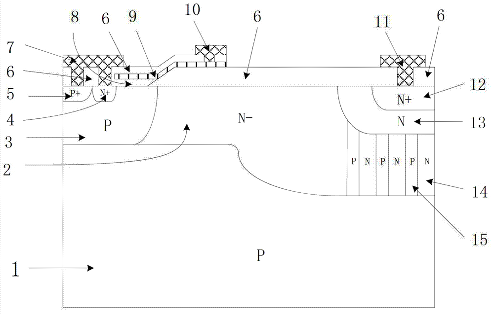
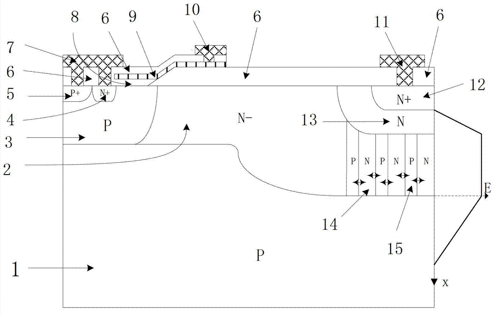
[0018] refer to figure 1 , an N-type vertical high-voltage lateral double-diffused metal-oxide-semiconductor transistor, comprising: a P-type silicon substrate 1, and an N-drift region 2, a P-type body region 3 and a P-type silicon substrate 1 are arranged on the P-type silicon substrate 1 Super junction structure, the super junction structure is composed of N-type regions 14 and P-type regions 15 which are alternately distributed in the direction of the connection drain region and the substrate, and the upper surface of the P-type silicon substrate 1 is an N-drift region 2 and a P-type body region. 3 and super junction structure coverage, an N-type source region 4, a P-type body contact region 5 and a gate oxide layer 8 are arranged above the P-type body region 3, an N-type buffer layer 13 is arranged above the N-drift region 2, An N-type drain region 12 is provided above the N-type buffer layer 13, a polysilicon gate 9 is provided above the gate oxide layer 8, an N-type sou...


PUM


Abstract

The invention relates to an N type longitudinal high-voltage tolerance transverse double diffused metal oxide semiconductor transistor. The N type longitudinal high-voltage tolerance transverse double diffused metal oxide semiconductor transistor comprises a P type silicon substrate, wherein an N-drift region and a P type body region are arranged on the P type silicon substrate, the upper surface of the P type silicon substrate is covered by the N-drift region and the P type body region, an N type source region, a P type body contact region and a gate oxide layer are arranged above the P type body region, an N type buffer layer is arranged above the N-drift region, an N type drain region is arranged above the N type buffer layer, a polysilicon gate is arranged above the gate oxide layer, a field oxide layer is arranged above the N type source region, the P type body contact region, the polysilicon gate, the N-drift region and the N type drain region, a first metal leading wire penetrating through the field oxide layer is connected on the N type source region and the P type body contact region, the polysilicon gate is connected with a second metal leading wire penetrating through the field oxide layer, and the N type drain region is connected with a third metal leading wire penetrating through the field oxide layer. The N type longitudinal high-voltage tolerance transverse double diffused metal oxide semiconductor transistor is characterized in that a hyperconjugation structure is arranged on the P type silicon substrate, and the hyperconjugation structure is constituted by N type regions and P type regions, which are alternately distributed in the direction of connecting the drain region with the substrate.

Description

technical field [0001] The present invention relates to the technical field of power semiconductor devices, in particular, to a lateral double-diffused metal-oxide-semiconductor transistor with a vertical super-junction structure at the drain end which improves the vertical withstand voltage. Background technique [0002] Power semiconductor devices are the basic elements for energy control and conversion in power electronic systems. The continuous development of power electronic technology has opened up a wide range of application fields for power semiconductor devices. Modern power electronic devices and related products represented by lateral double-diffused metal-oxide-semiconductor transistors with faster switching speed and wider safe operating area are used in the 4C industries represented by computers, communications, consumer electronics, and automotive electronics. play an important role. Today, power devices are developing in the direction of increasing operating...

Claims


Application Information

Patent Timeline
Patent Type & Authority Applications(China)
IPC IPC(8): H01L29/06H01L29/78
Inventor 祝靖林吉勇杨卓钱钦松孙伟锋陆生礼时龙兴
Owner SOUTHEAST UNIV
Features
  • R&D
  • Intellectual Property
  • Life Sciences
  • Materials
  • Tech Scout
  • Unparalleled Data Quality
  • Higher Quality Content
  • 60% Fewer Hallucinations
Learn More