Chained diffusion process for solar cell

A solar cell and diffusion process technology, applied in the directions of diffusion/doping, circuits, electrical components, etc., can solve the problems of difficult control of surface sheet resistance, low battery life, and high surface doping concentration, reducing the surface concentration The effect of too high, increasing production capacity and improving conversion efficiency

Inactive Publication Date: 2013-01-16
TIANWEI NEW ENERGY HLDG
View PDF8 Cites 9 Cited by
  • Summary
  • Abstract
  • Description
  • Claims
  • Application Information

AI Technical Summary

Problems solved by technology

[0007] The purpose of the present invention is to provide a chain diffusion process for solar cells, the purpose of this process is: 1. Solve the problems of high surface doping concentration caused by chain diffusion, low carrier life of the cell, and low conversion efficiency
2. Solve the problem that the surface square resistance caused by traditional wet etching and polishing is not easy to control, and the uniformity of square resistance after polishing is poor

Method used


Image

  • Chained diffusion process for solar cell

Examples


Embodiment 1

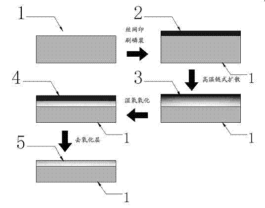
[0038] Such as figure 1 Shown.

[0039] A chain diffusion process for solar cells includes the following steps:

[0040] Step A: Use screen printing phosphor paste process for chain diffusion or spray phosphoric acid aqueous solution process for chain diffusion to form a screen printing surface phosphor paste layer 2 on the surface of the substrate silicon wafer 1;

[0041] Step B: After step A, perform high-temperature chain diffusion process to transform the screen-printed surface phosphor paste layer 2, and the formed P atoms diffuse into the surface of the base silicon wafer to form an N-type layer, and at the same time, the surface of the base silicon wafer is formed with Impurity layer, we collectively refer to the N-type layer and the impurity layer as the surface impurity distribution layer 3 after chain diffusion;

[0042] Step C: After step B, perform oxidation treatment on the surface of the surface impurity distribution layer 3 after chain diffusion, and quickly grow a un...

Embodiment 2

[0045] Such as figure 1 Shown.

[0046] Step A: Use the screen printing phosphor paste process for chain diffusion or spray the phosphoric acid aqueous solution process for chain diffusion to form a screen printing surface phosphor paste layer 2 on the surface of the substrate silicon wafer 1; the screen printing phosphor paste process performs chain diffusion The method of formula diffusion is to uniformly print the phosphor paste on the surface of the base silicon wafer 1 using a screen plate.

[0047] Step B: After step A, perform high-temperature chain diffusion process to transform the screen-printed surface phosphor paste layer 2, and the formed P atoms diffuse into the surface of the base silicon wafer to form an N-type layer, and at the same time, the surface of the base silicon wafer is formed with For the impurity layer, we collectively refer to the N-type layer and the impurity layer as the surface impurity distribution layer 3 after chain diffusion; the high temperatur...

Embodiment 3

[0051] The differences between this embodiment and Embodiment 1 and Embodiment 2 are:

[0052] The 1-square resistance of the base silicon wafer after step B is 5 ohm-30 ohm lower than the 1-square resistance of the base silicon wafer after step C.

[0053] The 1-square resistance of the base silicon wafer after step C is in the range of 60ohm-120ohm.


PUM


Abstract

The invention discloses a chained diffusion process for a solar cell. The chained diffusion process is to remove a highly-doped area on a diffused surface and improve the minority carrier lifetime of a diffused silicon wafer by growing a thick oxidation layer on the surface of a silicon wafer subjected to chained diffusion and washing off the oxidation layer, and comprises the following steps: making a reaction between steam and the diffused surface of the silicon wafer at a high temperature to quickly grow the thick oxidation layer in a short time; and finally, removing the oxidation layer. The chained diffusion process avoids the phenomenon that the ordinary diffusion process cannot avoid generating a 'dead layer', further reduces the surface concentration, improves the minority carrier lifetime and the conversion efficiency of the cell, and reduces the production cost of the solar cell.

Description

Technical field [0001] The invention relates to a production method of solar cells, in particular to a chain diffusion process for solar cells. Background technique [0002] At present, in the field of making P-type solar cell emitters, there are three commonly used methods. The first is to use phosphorus oxychloride (POCl 3 ) Liquid source diffusion, the second is chain diffusion after spraying phosphoric acid aqueous solution, and the third is chain diffusion after screen printing phosphorous paste. Among them, the first method has a simple process and is easy to operate, and can adjust the doping concentration and impurity distribution by adjusting the flux, diffusion temperature and process time, and has become a commonly used method in the field of solar cells. Although the latter two processes have the advantages of short process time, no complex loading and unloading devices, easy automatic production, and can be connected with texturing and etching processes to achieve a...

Claims


Application Information

Patent Timeline
Patent Type & Authority Applications(China)
IPC IPC(8): H01L31/18B41M1/12C30B31/06
CPCY02P70/50
Inventor 李质磊袁泽锐林洪峰张凤鸣盛雯婷
Owner TIANWEI NEW ENERGY HLDG
Why Eureka
Try Eureka