Method for reducing reflection of black silicon in wide band scope

A wide-band, anti-reflection technology, applied in sustainable manufacturing/processing, electrical components, climate sustainability, etc., to achieve low-cost, anti-reflection, and low-reflection effects

Active Publication Date: 2013-01-16
深圳市石金科技股份有限公司
View PDF4 Cites 17 Cited by
  • Summary
  • Abstract
  • Description
  • Claims
  • Application Information

AI Technical Summary

Problems solved by technology

[0006] The purpose of the present invention is to provide a method for reducing the surface reflectivity of silicon wafers in a wide range of wavelengths, so as to solve the problems in the prior art process

Method used


Image

  • Method for reducing reflection of black silicon in wide band scope
  • Method for reducing reflection of black silicon in wide band scope
  • Method for reducing reflection of black silicon in wide band scope

Examples


Embodiment 1

[0040] This embodiment provides a method for reducing the reflectivity of silicon wafers in a wide spectral range, including:

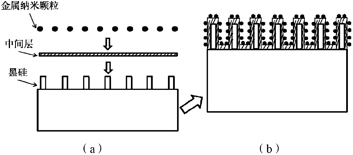
[0041] 1) Perform surface isolation and protection treatment on black silicon with nano-column structure, and deposit 30nm thick SiN on its surface by PECVD (that is, plasma chemical vapor deposition method) x middle layer;

[0042] 2) On the black silicon surface after the intermediate layer is prepared, Ag with a thickness of 5nm is deposited by thermal evaporation to obtain discontinuous Ag metal particles (above step 1) and 2) are reflected in image 3 a);

[0043] 3) Put the sample into an annealing furnace, blow nitrogen, and anneal at 200°C for 30 minutes to obtain Ag metal nanoparticles with more regular shape and uniform distribution, and the average diameter of Ag metal nanoparticles is about 25nm.

[0044] The schematic diagram of the black silicon-based surface plasmon wide-band anti-reflection structure obtained after the above steps is...

Embodiment 2

[0048] This embodiment provides a method for reducing the reflectivity of silicon wafers in a wide spectral range, including:

[0049] 1) Perform surface isolation protection treatment on black silicon with nanowire structure, and deposit 25nm thick SiN on its surface by PECVD x middle layer;

[0050] 2) On the black silicon after the intermediate layer was prepared, Ag with a thickness of 10nm was deposited by thermal evaporation to obtain discontinuous Ag metal particles;

[0051] 3) Put the sample into an annealing furnace, blow nitrogen, and anneal at 150°C for 20 minutes to obtain Ag metal nanoparticles with more regular shape and uniform distribution, and the average diameter of Ag nanoparticles is about 30nm.

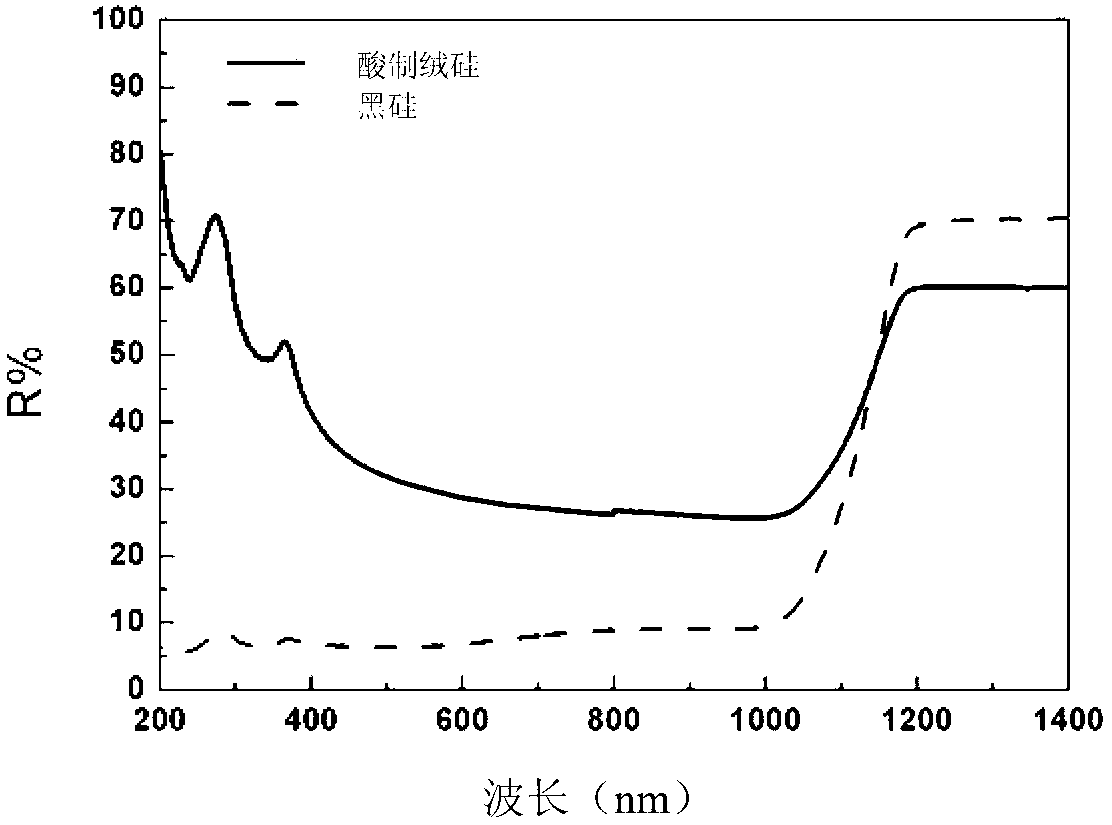
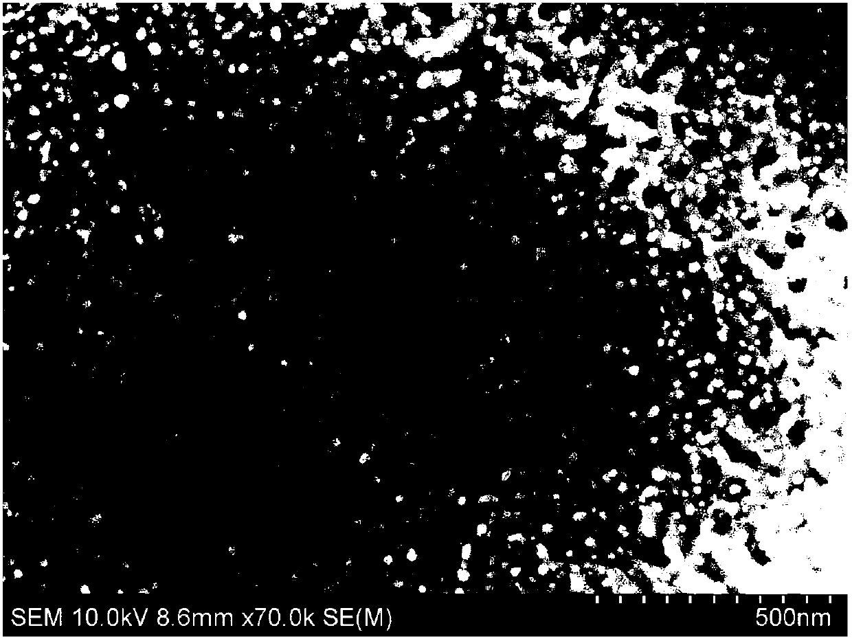
[0052] The SEM topography of the black silicon-based surface plasmon broadband anti-reflection structure obtained after the above steps is as follows Figure 7 shown. Figure 8 It is the reflectance spectrum of the polycrystalline silicon chip after the acid t...

Embodiment 3

[0054] This embodiment provides a method for reducing the reflectivity of silicon wafers in a wide spectral range, including:

[0055] 1) Carry out surface isolation and protection treatment on black silicon with nanoporous structure, and obtain SiO with a thickness of about 15nm after ozone oxidation for 30 minutes 2 middle layer;

[0056] 2) On the black silicon after the intermediate layer was prepared, Ag with a thickness of 10nm was deposited by thermal evaporation to obtain discontinuous Ag metal particles;

[0057] 3) Put the sample into an annealing furnace, and after vacuuming, anneal at 250°C for 60 minutes to obtain Ag metal nanoparticles with more regular shape and more uniform distribution.

[0058] The SEM topography of the black silicon-based surface plasmon wide-band anti-reflection structure obtained after the above steps is as follows: Figure 9 shown.


PUM

PropertyMeasurementUnit
thicknessaaaaaaaaaa
thicknessaaaaaaaaaa
diameteraaaaaaaaaa

Abstract

The invention provides a method for reducing reflection of black silicon in a wide band scope. The method comprises the following steps: 1) an intermediate layer is prepared on the surface of the black silicon, wherein the black silicon is silicon with a light trapping structure; 2) metal nanometer particles are deposited on the intermediate layer obtained in the step 1), and are not continuous or not in contact with one another; and 3) annealing processing is performed on a product obtained in the step 2). The method is simple in operation, low in cost, effectively combined with a black silicon technology, a surface isolation protection technology and a surface plasma technology to achieve a reflection reduction effect in the wide band scope, and conducive to the application in the industrial production of solar batteries.

Description

technical field [0001] The invention relates to a silicon anti-reflection method, more specifically, the method relates to a wide-band range anti-reflection method for black silicon, and the method is suitable for an anti-reflection layer in a silicon solar cell. Background technique [0002] As an indirect bandgap semiconductor material, silicon reflects more than 30% of sunlight. Therefore, anti-reflection structures or anti-reflection layers are an integral part of silicon solar cells. In traditional industry, monocrystalline silicon uses alkali anisotropic etching to obtain a pyramid structure, and its reflectivity is about 10%; polycrystalline silicon uses acid isotropic etching to obtain a "worm" structure, and its reflectivity is about 20%; Thereafter, one or more layers of anti-reflection coatings (SiN x , SiO 2 etc.) to achieve the effect of anti-reflection. However, these traditional methods of texturing cannot obtain a lower anti-reflection effect. [0003] I...

Claims


Application Information

Patent Timeline
Patent Type & Authority Applications(China)
IPC IPC(8): H01L31/18H01L31/0216
CPCY02P70/50
Inventor 王燕刘尧平叶大千梅增霞杜小龙
Owner 深圳市石金科技股份有限公司
Why Eureka
Try Eureka