Cathode isolating device for organic light emitting device and manufacturing method for cathode isolating device

A technology for organic light-emitting devices and isolation devices, which is applied in the manufacture of semiconductor/solid-state devices, electric solid-state devices, semiconductor devices, etc., can solve the problem of damage to organic functional layers or cathode materials, it is difficult to obtain high resolution, and it is not suitable for organic light-emitting devices. Cathode pattern and other problems, to save process steps, improve resolution, prevent cross effects

Inactive Publication Date: 2013-01-16
IRICO
View PDF6 Cites 5 Cited by
  • Summary
  • Abstract
  • Description
  • Claims
  • Application Information

AI Technical Summary

Problems solved by technology

However, the existing methods for making cathodes are not suitable for making cathode patterns of organic light-emitting devices
For example, chemicals used in

Method used


Image

  • Cathode isolating device for organic light emitting device and manufacturing method for cathode isolating device
  • Cathode isolating device for organic light emitting device and manufacturing method for cathode isolating device
  • Cathode isolating device for organic light emitting device and manufacturing method for cathode isolating device

Examples


Embodiment 1

[0024] A method for manufacturing a cathode isolation device for an organic light-emitting device, comprising the following steps:

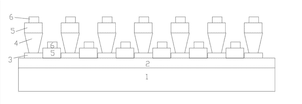
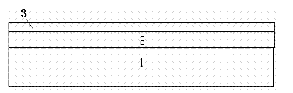
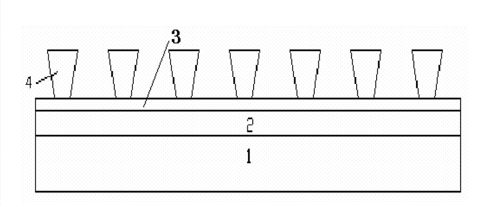
[0025] Such as figure 2 , 3 , 4, to make the cathode isolating device, first the ITO anode layer 2 on the glass substrate 1 is etched into the required pattern, and the cathode isolating device is made on the etched ITO anode layer 2, specifically coating The first layer of water-soluble insulating medium layer 3, after sintering, print the photosensitive insulating medium layer 4 on this layer, and then use the film graphic model as a mask to carry out photoetching to the photosensitive insulating medium layer 4, so that the photosensitive insulating medium Layer 4 forms an isolated band-like distribution with an inverted trapezoidal cross-section, and then uses the inverted trapezoidal pattern as a mask to wet-etch the water-soluble insulating medium to form an isolated band-like distribution with a rectangular cross-section, and finally stea...

Embodiment 2

[0031] After the glass substrate 1 is ultrasonically cleaned with acetone, the manufacturing process is carried out in the following steps:

[0032] 1. Etching the ITO anode layer 2 on the glass substrate 1 into the required pattern;

[0033] 2. The water-soluble insulating medium layer 3 is printed and dried (130°C, under the atmosphere, 15min);

[0034] 4. Sintering of the water-soluble insulating dielectric layer 3 (580°C, 20min in the atmosphere);

[0035] 5. The photosensitive insulating medium layer 4 is printed for the first time, and dried (100°C, under the atmosphere, for 15 minutes);

[0036] 6. The photosensitive insulating medium layer 4 is printed for the second time, and dried (100°C, under the atmosphere, for 15 minutes);

[0037] 7. Photolithography is performed on the photosensitive insulating medium layer 4 by using the film graphic model as a mask, the exposure energy is 800 mJ, and the developing solution is 0.3% sodium carbonate solution.

[0038] 8. Re...


PUM

PropertyMeasurementUnit
Widthaaaaaaaaaa
Thicknessaaaaaaaaaa
Viscosityaaaaaaaaaa

Abstract

The invention relates to a cathode isolating device for an organic light emitting device and a manufacturing method for the cathode isolating device. The cathode isolating device comprises a glass substrate (1), an ITO (indium tin oxide) anode layer (2), an organic material layer (5) and a cathode electrode layer (6). The cathode isolating device is characterized in that a water soluble insulating dielectric layer (3) and a light-sensitive insulating dielectric layer (4) are sequentially arranged between the ITO anode layer (2) and the organic material layer (5). Using the cathode isolating device can effectively isolate connection among metal electrodes to avoid short circuit and achieve the purpose of cathode separation, the bottom water soluble insulating dielectric layer is wide and can functionally take the place of a traditional internal insulating layer to achieve the purpose of isolation of the cathode from the anode, short circuit between the ITO anode and the metal cathode, especially short circuit and current leakage at the edges of the electrodes due to defects of pinholes and the like, can be prevented, and cross effect is effectively prevented by the design.

Description

technical field [0001] The invention relates to a cathode isolation device of an organic light-emitting device and a manufacturing method thereof. Background technique [0002] Organic light-emitting device is a new type of display device with excellent performance. It has the advantages of high brightness, high contrast, fast response, low driving voltage and full color, especially the simple manufacturing method and low cost. It is widely used in Small size flat panel display field. [0003] Generally speaking, an organic light-emitting device is a light-emitting device composed of a transparent conductive layer, an opaque conductive layer and one or more organic functional layers between them, and the functional stack is formed on a transparent substrate. The patterning of the transparent conductive layer forms a row of cathodes in the first direction, and the patterning of the opaque conductive layer forms a column of anodes in the second direction. The pixels of an or...

Claims


Application Information

Patent Timeline
IPC IPC(8): H01L51/52H01L51/56
Inventor 赵莉苏醒宇
Owner IRICO
Why Eureka
Try Eureka