Double-strain CMOS (Complementary Metal Oxide Semiconductor) integrated device and preparation method thereof

A dual-strain and device technology, which is applied in semiconductor/solid-state device manufacturing, electric solid-state devices, semiconductor devices, etc., can solve the problems of incompatibility in technology, wide application and development, difficulty in preparing large-diameter single crystals, and poor heat dissipation performance. Achieve the effect of improving electrical performance, suppressing short channel effect, and excellent circuit performance

Inactive Publication Date: 2015-04-22
XIDIAN UNIV
View PDF2 Cites 0 Cited by
  • Summary
  • Abstract
  • Description
  • Claims
  • Application Information

AI Technical Summary

Problems solved by technology

Although the frequency characteristics of GaAs and InP-based compound devices are superior, their preparation process is more complicated than that of Si, and the cost is high. 2 Such passivation layer and other factors limit its wide application and development.

Method used


Image

  • Double-strain CMOS (Complementary Metal Oxide Semiconductor) integrated device and preparation method thereof
  • Double-strain CMOS (Complementary Metal Oxide Semiconductor) integrated device and preparation method thereof
  • Double-strain CMOS (Complementary Metal Oxide Semiconductor) integrated device and preparation method thereof

Examples


Embodiment 1

[0050] Embodiment 1: prepare the double-strain CMOS integrated device and the circuit that the conduction channel is 45nm, concrete steps are as follows:

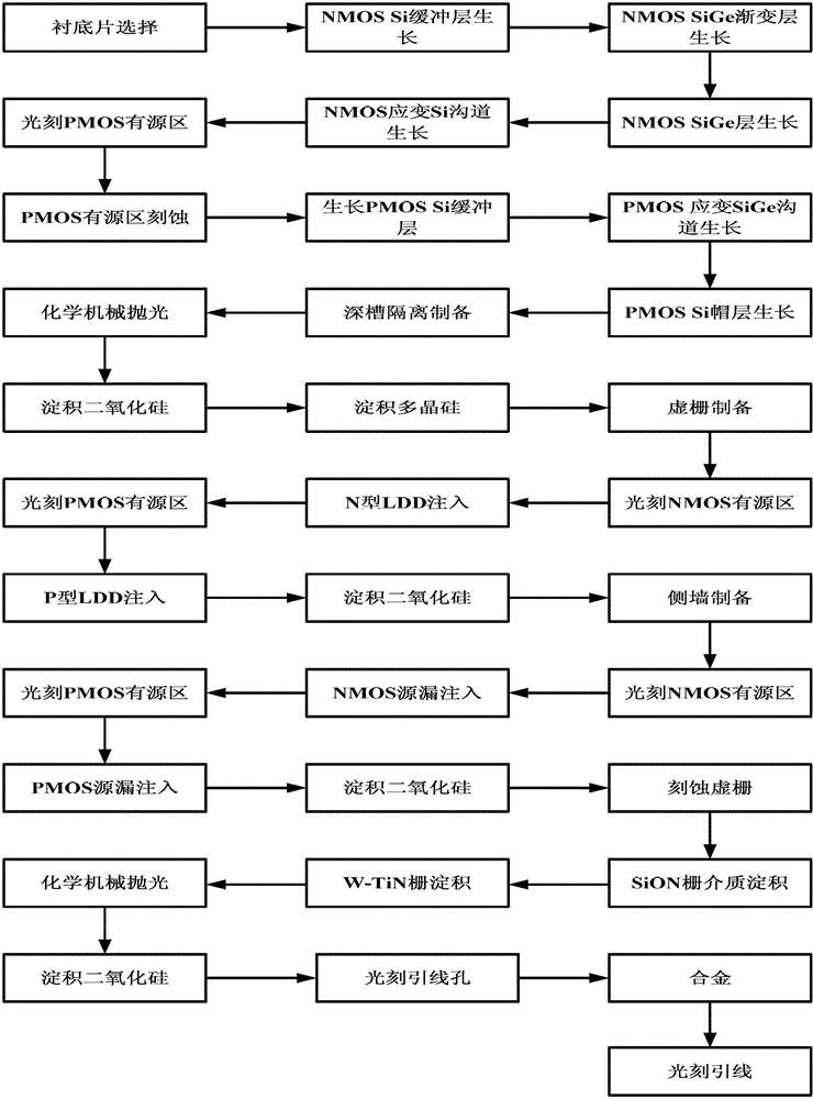
[0051] Step 1, NMOS epitaxial material preparation, such as figure 2 shown.

[0052] (1a) Select the doping concentration as 1×10 16 cm -3 A p-type Si substrate sheet 1;

[0053] (1b) Using chemical vapor deposition (CVD), grow a P-type Si buffer layer 2 with a thickness of 400 nm on the substrate at 600°C, with a doping concentration of 5×10 16 cm -3 ;

[0054] (1c) Using chemical vapor deposition (CVD), grow a P-type SiGe graded layer 3 with a thickness of 2 μm on the substrate at 600°C, with a bottom Ge composition of 0% and a top Ge composition of 15% , with a doping concentration of 5×10 16 cm -3 ;

[0055] (1d) Using the method of chemical vapor deposition (CVD), grow a P-type SiGe layer 4 with a thickness of 400nm on the substrate at 600°C, with a Ge composition of 15% and a doping concentration of 5×10 17...

Embodiment 2

[0091] Embodiment 2: The preparation of a dual-strain CMOS integrated device and circuit with a conductive channel of 30nm, the specific steps are as follows:

[0092] Step 1, NMOS epitaxial material preparation, such as figure 2 shown.

[0093] (1a) Select the doping concentration to be 5×10 15 cm -3 A p-type Si substrate sheet 1;

[0094] (1b) Using chemical vapor deposition (CVD), grow a P-type Si buffer layer 2 with a thickness of 300 nm on the substrate at 700°C, with a doping concentration of 1×10 16 cm -3 ;

[0095] (1c) Using the chemical vapor deposition (CVD) method, grow a P-type SiGe graded layer 3 with a thickness of 1.8 μm on the substrate at 700 ° C, the bottom Ge composition is 0%, and the top Ge composition is 20% %, the doping concentration is 1×10 16 cm -3 ;

[0096] (1d) Using chemical vapor deposition (CVD), grow a P-type SiGe layer 4 with a thickness of 300 nm on the substrate at 700 °C, with a Ge composition of 20% and a doping concentration of...

Embodiment 3

[0132] Embodiment 3: prepare the double-strain CMOS integrated device and the circuit that the conduction channel is 22nm, the specific steps are as follows:

[0133] Step 1, NMOS epitaxial material preparation, such as figure 2 shown.

[0134] (1a) Select the doping concentration as 1×10 15 cm -3 A p-type Si substrate sheet 1;

[0135] (1b) Using chemical vapor deposition (CVD), grow a P-type Si buffer layer 2 with a thickness of 200 nm on the substrate at 750°C, with a doping concentration of 5×10 15 cm -3 ;

[0136] (1c) Using chemical vapor deposition (CVD), grow a P-type SiGe graded layer 3 with a thickness of 1.5 μm on the substrate at 750°C, with a bottom Ge composition of 0% and a top Ge composition of 25% %, the doping concentration is 5×10 15 cm -3 ;

[0137] (1d) Using chemical vapor deposition (CVD), grow a P-type SiGe layer 4 with a thickness of 200 nm on the substrate at 750°C, with a Ge composition of 25% and a doping concentration of 5×10 16 cm -3 ;...


PUM

PropertyMeasurementUnit
thicknessaaaaaaaaaa
thicknessaaaaaaaaaa
thicknessaaaaaaaaaa

Abstract

The invention discloses a double-strain CMOS (Complementary Metal Oxide Semiconductor) integrated device and a preparation method thereof. The method comprises the following steps: growing a P-type Si epitaxial layer, a P-type gradient SiGe layer and the like as NMOS (N-channel Mental Oxide Semiconductor) construction material layers continuously on a substrate, etching a PMOS (P-channel Metal Oxide Semiconductor) active area deep trench, epitaxially growing an N-type Si layer and the like as a PMOS active area selectively in the trench, and preparing the deep-trench isolator between the NMOS and the PMOS; depositing SiO2 and Poly-Si on the surface of the substrate, preparing a virtual grid electrode, depositing SiO2, preparing a side wall, and implanting N-type ions in a self-aligning manner to form the source drains of NMOS and PMOS; depositing SiO2, etching a virtual grid, depositing an SiON grid dielectric layer, and depositing a W-TiN composite grid to form the double-strain CMOS integrated device. According to the method, the tension strain Si with high electron mobility and the compression strain SiGe with high hole mobility are fully utilized as conducting channels, and the performances of the CMOS integrated device and circuits are efficiently improved.

Description

technical field [0001] The invention belongs to the technical field of semiconductor integrated circuits, and in particular relates to a double-strain CMOS integrated device and a preparation method. Background technique [0002] In the 20th century, the rapid development of the semiconductor industry promoted the process of knowledge and informatization of the entire human society, and at the same time changed the way of thinking of human beings. It not only provides humans with a powerful tool to transform nature, but also opens up a broad space for development. Therefore, semiconductor integrated circuits have become the basis for the development of the electronics industry. In the past few decades, the rapid development of the electronics industry has had a huge impact on social development and national economy. At present, the electronics industry has become the largest industry in the world, occupying a large share in the global market, and its output value has exceed...

Claims


Application Information

Patent Timeline
Patent Type & Authority Patents(China)
IPC IPC(8): H01L27/06H01L21/28H01L21/8249H01L29/06
Inventor 胡辉勇宋建军宣荣喜张鹤鸣王斌王海栋郝跃
Owner XIDIAN UNIV
Why Eureka
Try Eureka