

Fluorescence sensor
A fluorescent sensor and light quantity technology, applied in the field of fluorescent sensors, can solve the problems of shortening the life of the sensor and fast deterioration of the indicator
- Summary
- Abstract
- Description
- Claims
- Application Information
AI Technical Summary
Problems solved by technology
Method used
Image

Examples
no. 1 approach
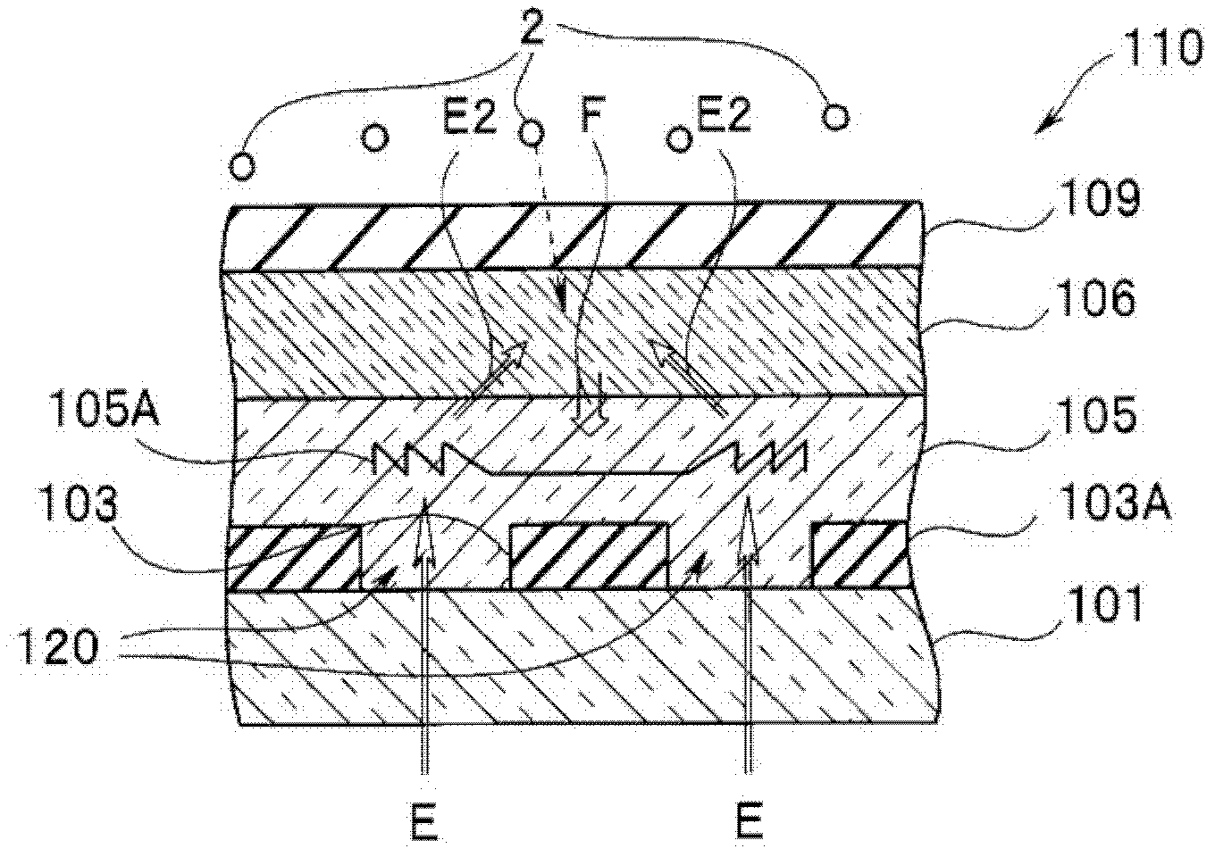
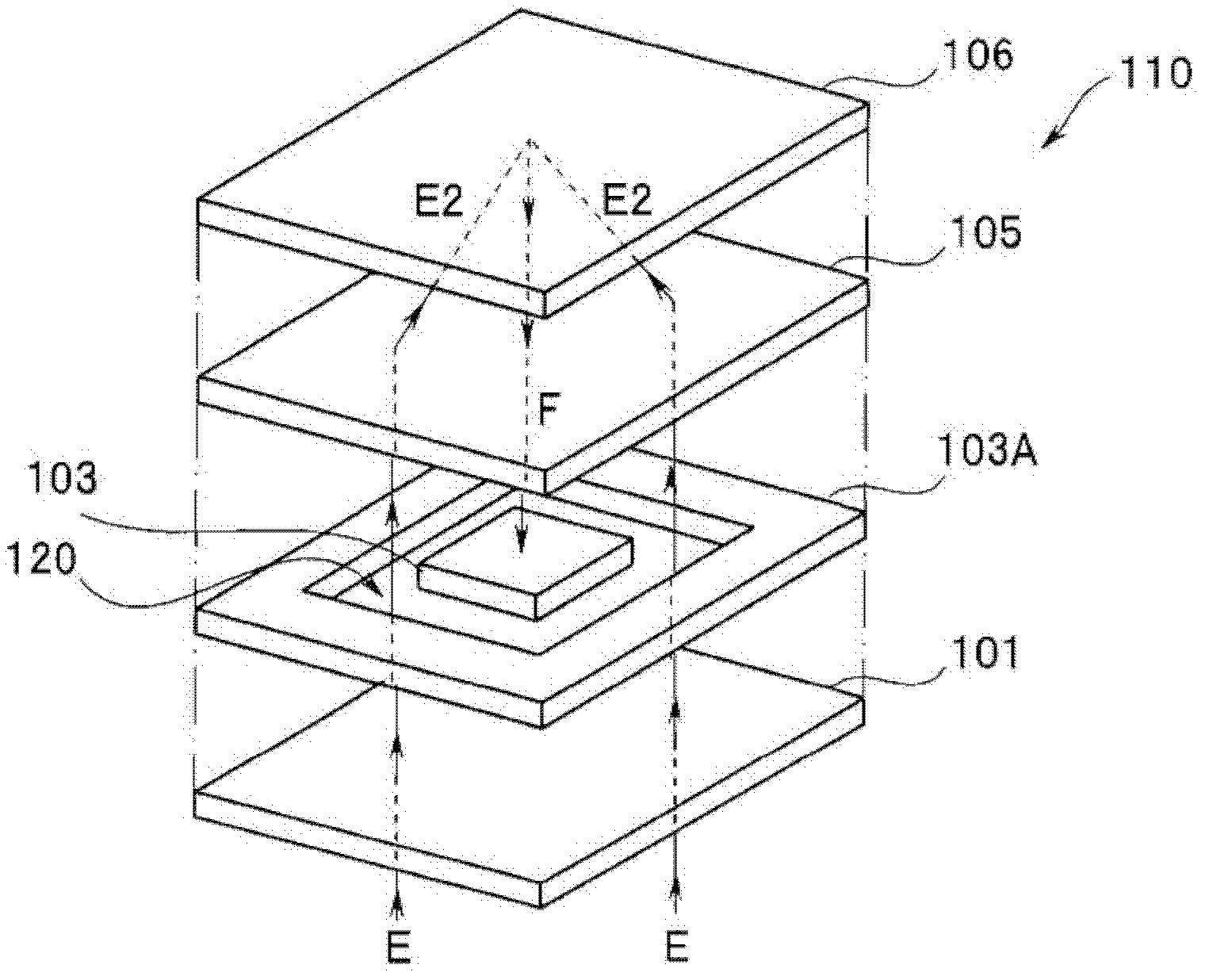
[0027] Next, a fluorescence sensor 10 according to a first embodiment of the present invention will be described with reference to the drawings. Such as image 3 and Figure 4 As shown, the fluorescence sensor 10 of this embodiment has: a silicon substrate 11 as a main substrate; and a light emitting element substrate ( Hereinafter referred to as "LED substrate") 15, transparent resin layer 16, indicator layer 17, and light-shielding layer 18, in which the reflective film 20 is a light-quantity equalization portion that makes the light-quantity distribution of emitted excitation light uniform. A photodiode element (hereinafter referred to as “PD element”) 12 as a photoelectric conversion element is formed on a silicon substrate 11 . A light-emitting diode element (hereinafter referred to as "LED element") 15C, which is a light-emitting element that generates excitation light E, is formed substantially at the center of first principal surface 15A of LED substrate 15 through w...
no. 2 approach
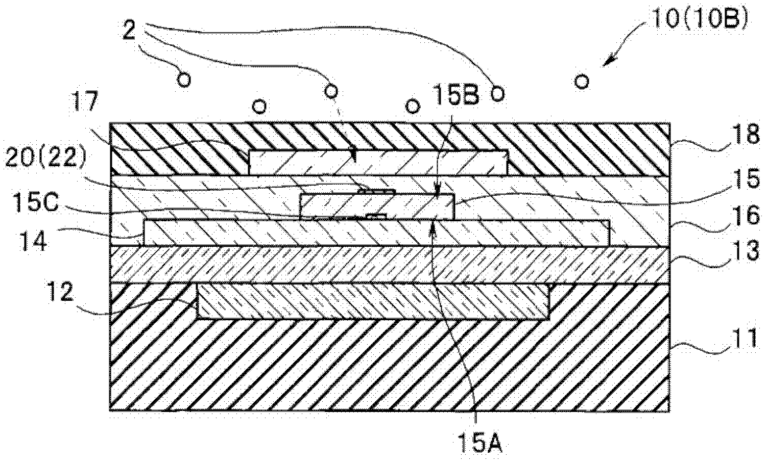
[0070]Next, a fluorescence sensor 10B according to the second embodiment will be described. Since the fluorescence sensor 10B is similar to the fluorescence sensor 10 , the components with the same functions are given the same numerals and their descriptions are omitted. The light quantity equalizing portion of the fluorescence sensor 10B is a light-shielding film 22 formed on at least a region of the second main surface 15B facing the LED element 15C and having a function of absorbing excitation light. The light-shielding film 22 is an excitation light attenuation portion that attenuates the light intensity in a region where the light intensity distribution has a large light intensity.
[0071] That is, if Figure 9 As shown, compared with the case of "(A) without a light-shielding film", in the case of "(B) with a reflective film", the amount of light in the central area decreases, while the amount of light in the peripheral area does not change. The light-shielding film 2...
no. 3 approach
[0075] Next, a fluorescence sensor 10C according to the third embodiment will be described. Since the fluorescence sensor 10C is similar to the fluorescence sensor 10 , components with the same functions are assigned the same numerals and descriptions thereof are omitted.
[0076] Such as Figure 10 As shown, the fluorescence sensor 10C has a main substrate 25 having a recess 33 , an LED substrate 15 provided with a reflective film 20 , a transparent resin layer 16C, an indicator layer 17C, and a light shielding layer 18C. The LED substrate 15 , the transparent resin layer 16C, and the indicator layer 17C are disposed inside the recess 33 , and the light-shielding layer 18C is disposed so as to close the opening of the recess 33 .
[0077] The main substrate 25 is manufactured by bonding a wiring substrate 30 having various wiring layers not shown and a rectangular prism-shaped frame-shaped substrate 40 having a through hole in the center. Therefore, in the main substrate 25...
PUM
| Property | Measurement | Unit |
|---|---|---|
| Diameter | aaaaa | aaaaa |
Abstract
Description
Claims
Application Information