Metal dielectric film wideband pulse compressed grating
A metal medium, broadband pulse technology, applied in diffraction grating and other directions, to achieve the effect of high diffraction efficiency and high damage threshold
- Summary
- Abstract
- Description
- Claims
- Application Information
AI Technical Summary
Problems solved by technology
Method used
Image
Examples
Embodiment 1
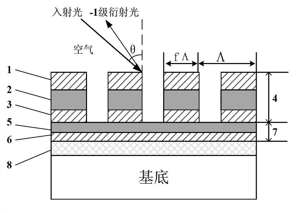
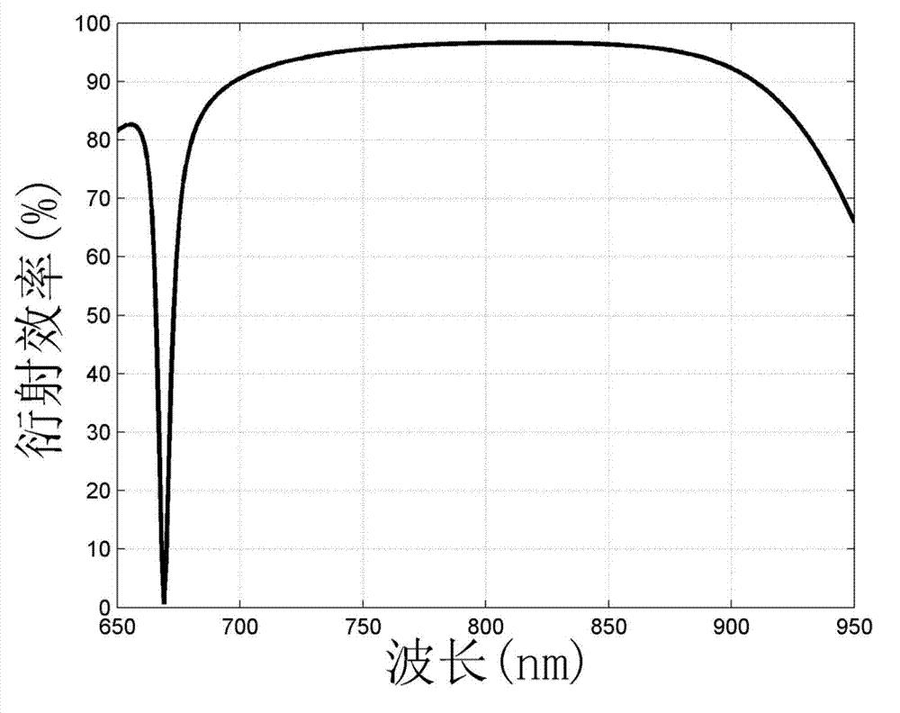
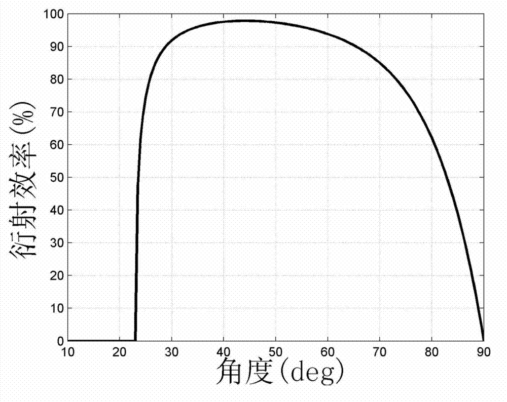
[0027] The metal dielectric film pulse compression grating is composed of a quartz substrate, a metal layer 8, a matching layer 7 composed of two dielectric films and a rectangular etching layer 4. The period of the rectangular etching layer 4 is 574.7 nanometers, the duty ratio is 0.26, and the SiO of the third low refractive index film layer 1 2 (refractive index 1.45) thickness 100 nanometers, the material of the second high refractive index film layer 2 is HfO 2 (refractive index 1.96) layer thickness 149 nm, second low refractive index film layer 3 SiO 2 The thickness is 57nm. The first high refractive index layer 5 of the matching layer 7 is HfO 2 , with a thickness of 119 nanometers; the first low refractive index layer 6 is SiO2, with a thickness of 81 nanometers. The gold layer 8 has a thickness of 200 nm. Such as figure 2 When the incident angle is 53°, for the incident light of 800 nm, the -1 order diffraction efficiency of the grating TE is the highest, great...
PUM
 Abstract
Description
Claims
Application Information


