High-reflection film for 10 kW semiconductor laser and preparation method thereof

A high-reflection film and laser technology, applied in the field of optical reflective films, can solve the problems of increasing the difficulty of film thickness monitoring, increasing the number of film layers, and increasing the cost of coating, so as to improve the ability to resist laser damage and reduce the number of film layers. number, the effect of reducing the plating time

Inactive Publication Date: 2019-11-12
DONGGUAN UNIV OF TECH +1
View PDF6 Cites 5 Cited by
  • Summary
  • Abstract
  • Description
  • Claims
  • Application Information

AI Technical Summary

Problems solved by technology

[0003] The traditional dielectric high-reflection film uses two kinds of high and low refractive index materials superimposed, and the optical thickness is λ / 4 periodic multilayer film structure. It is known from the theory of thin film optics that if the given number of layers is an odd number and the high refractive index layer is used as the The outermost layer can always get the maximum reflectivity, so the basic reflective film stack structure is generally Sub / (HL) S H / Air; the reflectivity increases with the increase of film thickness, so in order to obtain high reflectivity, you can choose a material combination with a large difference between high and low refractive index and deposit more layers. Theoretically speaking, the all-dielectric film layer When the number of layers is sufficient, a reflectivity close to 100% can be achieved, but in fact the number of layers of the film cannot be increased infinitely, and the highest achievable reflectivity is limited by the absorption and scattering loss of the film layer, and the more layers More, the greater the stress of the film layer, the difficulty of film thickness monitoring will increase, and the plating cost will also increase accordingly

Method used


Image

  • High-reflection film for 10 kW semiconductor laser and preparation method thereof

Examples


preparation example Construction

[0032] The preparation method of the high reflection film provided by the invention comprises the following steps:

[0033] S1. cleaning the substrate;

[0034] S2. Clean the reaction chamber, place the substrate and the coating material in the coating equipment, and vacuumize to 10 -4 Below Pa;

[0035] S3. Set the control program of the coating equipment, and prepare TiO on the substrate in turn 2 - SiO 2 Membranes and HfO 2 - SiO 2 Membrane stack, and coated with HfO on the outermost layer 2 film layer;

[0036] Among them, the TiO 2 For the film layer, the substrate temperature is 280-350°C; 2 For the film layer, the substrate temperature is 200-260°C; HfO plating 2 For the film layer, the substrate temperature is 380-430°C;

[0037] S4. Annealing the plated film in situ at 300-400° C. for 20-60 min to prepare the high-reflection film.

[0038] What the substrate of the present invention adopts is K9 glass, and its anti-laser damage property is better than SiO ...

Embodiment 1

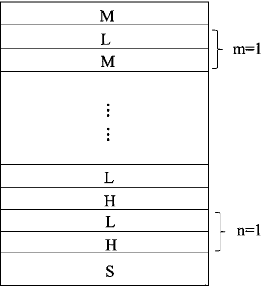
[0043] A high-reflection film for a 10kW semiconductor laser is characterized in that it includes a substrate and an optical film system attached to the substrate, and its characteristic structure is S / (HL) 10 (ML) 3 M / Air, where S means K9 glass, H means TiO with high refractive index 2 film layer, L means SiO with low refractive index 2 film layer, M indicates HfO with high damage threshold 2 film layer; the high reflection film is a laser high reflection film with a working wavelength λ of 1064 nm, and the preparation method is as follows:

[0044] S1. The substrate is cleaned, and on the ultra-clean bench, use a non-woven cloth dipped in a mixed solution of alcohol and ether (mixing ratio 3:1) to clean the substrate, and then dry it;

[0045] S2. Fully clean the reaction chamber, keep the equipment with a high degree of cleanliness, place the cleaned substrate and coating material in the ion beam-assisted deposition coating equipment, and vacuum to 10 -4 Below Pa;

[...

Embodiment 2-8

[0055] Embodiment 2-8 is compared with embodiment 1, and difference is that described TiO 2 - SiO 2 Films and HfO 2 - SiO 2 The period number of the film system is shown in Table 1, and the others are the same as in Example 1. Table 1 also shows the reflectivity and anti-laser damage threshold of the high-reflection film prepared in Example 2-5 at λ = 1064 nm.

[0056] It can be seen from the test results in Table 1 that when HfO 2 - SiO 2 When the period of the film system is constant, as the TiO 2 - SiO 2 The period number of the film system increases, the reflectivity of the high-reflection film increases, but the damage threshold decreases, because the high refractive index of TiO 2 The number of film layers increases, so the reflectivity increases, but as the number of film layers increases, the HfO 2 The relative thickness of the number of film layers is reduced, so the anti-laser damage threshold is reduced, and TiO 2 - SiO 2 When the period number of the film ...


PUM

PropertyMeasurementUnit
wavelengthaaaaaaaaaa
thicknessaaaaaaaaaa

Abstract

The invention discloses a high-reflection film for a 10 kW semiconductor laser and a preparation method thereof. A HfO2-TiO2-SiO2 multi-material film structure and the characteristic of large refractive index difference of aTiO2-SiO2 film combination are used to meet the requirement of high reflectivity under a few layers; the HfO2-SiO2 material has the characteristic of high laser damage resistance threshold, and a HfO2-SiO2 film stack is superimposed on the outermost part of the TiO2-SiO2 film stack, thereby improving the half-wave protection effect of laser damage resistance on TiO2-SiO2, achieving a few film layers, meeting the requirement of high reflectivity and improving the laser damage resistance of the film; the high-reflection film is prepared by ion beam assisted deposition, ametallic hafnium target, a metallic titanium target and a quartz glass sheet are used as coating materials, and the evaporation film is bombarded with an oxygen ion beam to obtain an oxide film, so that the compactness and stability of the film are improved.

Description

technical field [0001] The invention belongs to the technical field of optical reflection films, in particular to a high reflection film for a 10 kW semiconductor laser and a preparation method thereof. Background technique [0002] Due to its good coherence, monochromaticity, high brightness and directivity, lasers are widely used in precision measuring instruments, photoelectric pod systems, low-light night vision systems, communications and information transmission, military, national defense and other fields. Optical components are used as One of the key foundations of laser technology has an irreplaceable position in the laser system, and it is also the most vulnerable to laser damage, so the ability of optical components to resist laser damage directly determines the effective output power of the laser in the entire laser system. Low; therefore, with the continuous improvement of laser output power and energy, higher and higher requirements are put forward for the refl...

Claims


Application Information

Patent Timeline
Patent Type & Authority Applications(China)
IPC IPC(8): G02B5/08C23C14/24C23C14/58C23C14/10C23C14/08
CPCC23C14/0021C23C14/083C23C14/10C23C14/24C23C14/5806G02B5/0816
Inventor 郭建文王瑾邓君李小婷孙振忠朱宝华路崧赵曙明王皓亮
Owner DONGGUAN UNIV OF TECH
Why Eureka
Try Eureka