Preparation method of light emitting diode with photonic crystals with gradually-changed radius

A technology of light-emitting diodes and photonic crystals, which is applied in semiconductor devices, electrical components, circuits, etc., can solve the problems of low external quantum efficiency of light-emitting diodes, low light extraction efficiency, and restricting the development of light-emitting diodes.

Inactive Publication Date: 2013-02-13
INST OF SEMICONDUCTORS - CHINESE ACAD OF SCI
View PDF4 Cites 6 Cited by
  • Summary
  • Abstract
  • Description
  • Claims
  • Application Information

AI Technical Summary

Problems solved by technology

[0003] However, the total internal reflection at the interface between the light-emitting diode and the outside air makes the external quantum efficiency of the light-emitting diode very low, and most of the light emitted by the active region is confined inside the light-emitting diode. develop

Method used


Image

  • Preparation method of light emitting diode with photonic crystals with gradually-changed radius
  • Preparation method of light emitting diode with photonic crystals with gradually-changed radius
  • Preparation method of light emitting diode with photonic crystals with gradually-changed radius

Examples


Embodiment Construction

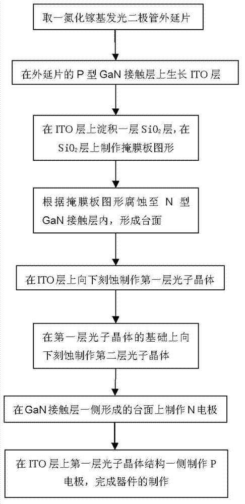
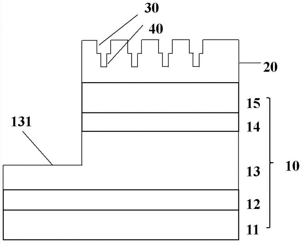
[0018] see figure 1 and refer to Figure 2-Figure 5 Shown, the present invention provides a kind of preparation method of photonic crystal light-emitting diode of gradual change radius, comprises the following steps (referring to figure 1 ):

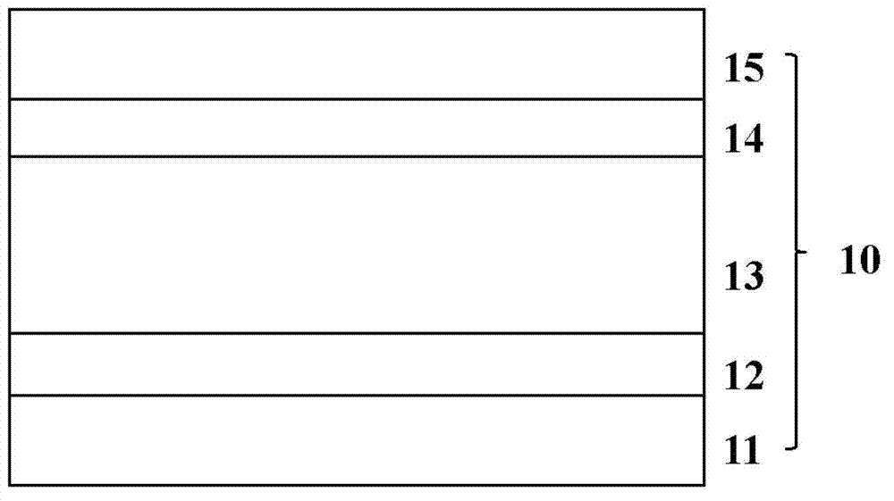
[0019] Step 1: Take a gallium nitride-based light-emitting diode epitaxial wafer 10, the epitaxial wafer 10 includes a GaN buffer layer 12 grown sequentially on a substrate 11 by metalorganic chemical vapor deposition or suspended epitaxial wafer technology, an N-type GaN contact Layer 13, active layer 14 and P-type GaN contact layer 15, the material of substrate substrate 11 in this epitaxial wafer 10 is sapphire, silicon, ZnO or SiC (see figure 2 );

[0020] Step 2: On the P-type GaN contact layer 15 of the epitaxial wafer 10, grow an ITO layer 20 by magnetron sputtering, evaporation, chemical vapor deposition or thermal spraying. The ITO layer has been alloyed to have low resistivity and high light transmission Efficiency charact...


PUM


Abstract

The invention provides a preparation method of a light emitting diode with photonic crystals with gradually-changed radiuses, comprising the following steps of: obtaining a gallium nitride based light emitting diode epitaxial wafer; growing an ITO (Indium Tin Oxide) layer on a P-type GaN contact layer of the epitaxial wafer; depositing a SiO2 layer on the ITO layer; manufacturing a mask plate graph on the SiO2 layer; etching according to the mask plate graph to remove one part of the SiO2 layer, the P-type GaN contact layer, an active layer and an N-type GaN contact layer at one side of the epitaxial wafer; etching until the depth is in the N-type GaN contact layer; etching downwards and manufacturing a first photonic crystal layer structure on the ITO layer, and etching downwards and manufacturing a second photonic crystal layer structure on the basis of the first photonic crystal layer structure, wherein the second photonic crystal layer structure is the same as the first photonic crystal layer structure in a lattice constant; manufacturing an N-electrode on a tabletop formed at one side of the GaN contact layer; and manufacturing a P-electrode at one side of the first photonic crystal layer structure on the ITO layer to finish the manufacturing of a device. According to the preparation method disclosed by the invention, the light extraction efficiency of the light emitting diode is improved.

Description

technical field [0001] The invention relates to the technical field of semiconductors, in particular to a method for preparing a photonic crystal light-emitting diode with a gradual radius that can improve light extraction efficiency. Background technique [0002] GaN-based light-emitting diodes have the advantages of long life, high brightness, small size, energy saving, and shock resistance. It is the core part of manufacturing white light-emitting diodes. Recently, the National Development and Reform Commission issued a report on prohibiting the sale and export of incandescent lamps. Many departments and local governments began to vigorously promote LED lighting. In 2012, the State Council arranged 2.2 billion yuan to support the promotion of energy-saving lamps and LED lamps. [0003] However, the total internal reflection at the interface between the light-emitting diode and the outside air makes the external quantum efficiency of the light-emitting diode very low, and ...

Claims


Application Information

Patent Timeline
Patent Type & Authority Applications(China)
IPC IPC(8): H01L33/20
Inventor 许兴胜王华勇高永浩
Owner INST OF SEMICONDUCTORS - CHINESE ACAD OF SCI
Why Eureka
Try Eureka