Eureka AIR delivers breakthrough ideas for toughest innovation challenges, trusted by R&D personnel around the world.

Insulating board for circuit board production, circuit board and circuit board production method

A production method and circuit board technology, applied in the directions of printed circuits, printed circuit manufacturing, printed circuit components, etc., can solve the problems of many processing procedures, short circuits, and complicated etching processes.

Active Publication Date: 2013-02-13
GUANGDONG SHENGYI SCI TECH
View PDF3 Cites 13 Cited by
  • Summary
  • Abstract
  • Description
  • Claims
  • Application Information

AI Technical Summary

Problems solved by technology

[0007] 1. The process is complicated and the production cost is high: because this production process is to first produce a circuit board with copper foil covering the upper and lower surfaces of the entire board, and then print the circuit pattern required by the PCB on the circuit board and correspondingly etch the required circuit. This production process is quite complicated, and it is more difficult for complex wiring arrangements in the production process, resulting in high production costs of the entire PCB;
[0008] 2. Low precision and high defective rate: due to the manual etching according to the circuit pattern, the accuracy of the whole production is not easy to be guaranteed, and the defective rate is high, especially as emerging electronic products refine the circuit and the plate material Thinning requirements are constantly increasing, and it is difficult to achieve better precision with this process, and the strength of the etched wires is also very low, which is likely to cause defects such as circuit short circuits;
[0009] 3. Low production efficiency: the etching process is relatively complicated, and it is all operated manually, which makes the entire production efficiency very low;
[0010] 4. Waste of energy and high material cost: a large amount of conductive metal (copper foil) is wasted during the etching process, which makes the material cost high;
[0011] 5. There are many processing procedures after etching: after the circuit board is etched, the circuit board needs to be cleaned, and the circuit board needs to be dried after cleaning, which undoubtedly increases the operation process, increases the production cost, and reduces the production efficiency. And the cleaned water also needs to be treated, because the cleaned water also contains recyclable metals and etching solutions. If it is discharged directly, it will not only waste resources but also pollute the environment. Therefore, the cleaned water must be treated, which will cause Complicated process;
[0012] 6. The subsequent treatment of the etching solution is complicated: the solution after etching contains some conductive metals. If it is not treated and discharged directly, the metal in the solution will be wasted on the one hand, and on the other hand it will cause serious pollution to the environment. If the solution is Treatment requires not only the extraction of metals from the solution, but also the extraction of other elements that are harmful to the environment in the solution, which can only be discharged after meeting the environmental protection requirements, which complicates the subsequent treatment of the etching solution;
[0013] 7. The substrate cutting process is complicated: the insulating substrate in the subtractive process is still produced according to the original substrate process, and every time a circuit board is mass-produced, the size of the circuit board produced is very small , so it is necessary to cut several substrates of the same size from a large substrate, which increases the production process and operation difficulty
When using this method to produce circuit boards, when the circuit distribution is relatively dense, the only way to reduce the line width of the wires is to ensure that there is no short circuit between the circuits. However, after the line width of the wires is reduced, the strength of the wires cannot meet the requirements. It does not short-circuit and meets the necessary strength of the wire. Those skilled in the art increase the height of the wire, but this operation not only increases the difficulty of wire layout, but also the wire is easy to fall off, which will also cause a short circuit on the circuit board.

Method used


Image

  • Insulating board for circuit board production, circuit board and circuit board production method
  • Insulating board for circuit board production, circuit board and circuit board production method
  • Insulating board for circuit board production, circuit board and circuit board production method

Examples


Embodiment 1

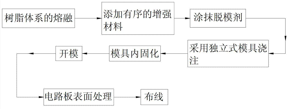
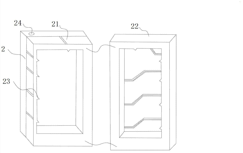
[0132] Such as figure 2 with 3 As shown, in this embodiment, the resin system adopts phenolic resin in the thermosetting resin, and the mold adopts a casting mold, and the casting mold is selected as image 3 Shown free-standing mold 2, its concrete production method comprises the following steps:

[0133] The first step: the melting of the resin system, the resin system is physically mixed, mixed evenly and then heated up to semi-cure, and the resin system is kept in a molten state after semi-cured to a certain extent;

[0134]Step 2: add orderly reinforcing materials, and orderly hang the reinforcing materials in the independent mold 2;

[0135] The third step: apply a release agent, apply a release agent to the side of the independent mold 2 in contact with the resin system,

[0136] Wherein, the structure of independent mold 2 is as image 3 As shown, it includes an upper mold 21 and a lower mold 22. The upper mold 21 and the lower mold 22 have a cavity for containing...

Embodiment 2

[0145] Such as Figure 4 with 5 As shown, in this embodiment, the resin system adopts the phenolic resin in the thermosetting resin, and the mold adopts a compression mold, where the compression mold is selected as Figure 5 Shown free-standing mold 3, its concrete production method comprises the following steps:

[0146] The first step: the melting of the resin system, the resin system is physically mixed, mixed evenly and then heated up to semi-cure, and the resin system is kept in a molten state after semi-cured to a certain extent;

[0147] Step 2: Add disordered reinforcing materials, add reinforcing materials to the molten resin system, and stir evenly with a stirring tool;

[0148] The third step: the mixture of the resin system and the reinforcing material forms a sheet or a block;

[0149] Step 4: apply a release agent, apply a release agent to the side of the independent mold 3 in contact with the resin system,

[0150] Wherein, the structure of independent mold ...

Embodiment 3

[0160] Such as Image 6 with 12 As shown, in this embodiment, the resin system adopts polyvinyl chloride in thermoplastic resin, and the mold adopts a pouring mold, and the pouring mold is selected such as Figure 7-12 As shown in the assembled mold 4, its specific production method comprises the following steps:

[0161] The first step: the melting of the resin system, the resin system is physically mixed, the temperature is raised after mixing evenly, and the molten state of the resin system is maintained;

[0162] Step 2: Add disordered reinforcing materials, add reinforcing materials to the molten resin system, and stir evenly with a stirring tool;

[0163] The third step: apply a release agent, apply a release agent to the side of the assembled mold 4 in contact with the resin system,

[0164] Wherein, the structure of assembled mold 4 is as follows Figure 7-12 Shown, comprise the first mold 41, the second mold 42, the third mold 43, the fourth mold 44 and the fifth ...


PUM


Abstract

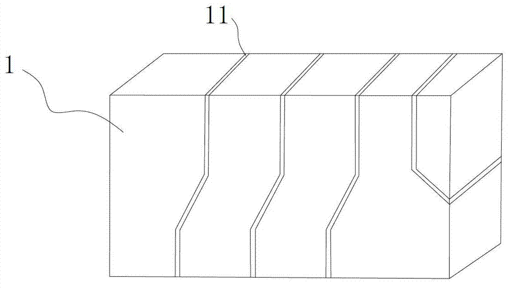
The invention discloses an insulating board for circuit board production. The insulating board is provided with wiring patterns, and the whole insulating board is molded through mold pouring or mold pressing by adopting a resin system with specific form in one time. The invention further discloses a circuit board which adopts the insulating board, and conducting materials are filled on the wiring patterns of the insulating board. The invention further discloses a circuit board production method which produces the circuit board, the method comprises the following steps: adopting the resin system with specific form; adopting a mold matched with the appearance of the circuit board and the wiring patterns on the circuit board; placing the resin system into the mold; by means of the mold, directly pouring or mold-pressing the appearance of the circuit board and the wiring patterns on the circuit board; and filling the conducting materials on the wiring patterns to form circuit board conducting patterns. The mold is adopted to directly mold the circuit board, thereby enabling the whole circuit board manufacture technology to be simplified in process, lowering production cost and improving production accuracy and efficiency.

Description

technical field [0001] The invention relates to the technical field of circuit board manufacturing, in particular to an insulating board for producing a circuit board, a circuit board containing the insulating board, and a method for producing the circuit board. Background technique [0002] PCB (Printed Circuit Board), the Chinese name is printed circuit board, also known as printed circuit board, printed circuit board, is an important electronic component, a support for electronic components, and a provider of electrical connections for electronic components. Because it is made using electronic printing, it is called a "printed" circuit board. [0003] At present, the printed circuit PCB manufacturing process is mainly divided into additive method and subtractive method. In my country, the PCB manufacturing process applied on a large scale is the PCB subtractive method. The subtractive method is a method of selectively removing part of the copper foil on the surface of th...

Claims


Application Information

Patent Timeline
Patent Type & Authority Applications(China)
IPC IPC(8): H05K3/00H05K3/10H05K1/02B29C39/02B29C43/02
Inventor 苟铭刘熙苏晓声李龙飞
Owner GUANGDONG SHENGYI SCI TECH
Why Eureka
Eureka Blog
Learn More