Preparation method of wide-forbidden-band semiconductor flexible substrate

A wide-bandgap semiconductor and flexible substrate technology, applied in the field of microelectronics, can solve the problems of high manufacturing cost and small crystal size, and achieve the effect of improving crystal quality, large substrate size, and easy industrialization

Active Publication Date: 2013-02-27
HUNAN RED SUN PHOTOELECTRICITY SCI & TECH
View PDF4 Cites 12 Cited by
  • Summary
  • Abstract
  • Description
  • Claims
  • Application Information

AI Technical Summary

Problems solved by technology

In addition, the substrate can also solve the problems of high manufacturing cost...

Method used


Image

  • Preparation method of wide-forbidden-band semiconductor flexible substrate
  • Preparation method of wide-forbidden-band semiconductor flexible substrate
  • Preparation method of wide-forbidden-band semiconductor flexible substrate

Examples


Embodiment 1

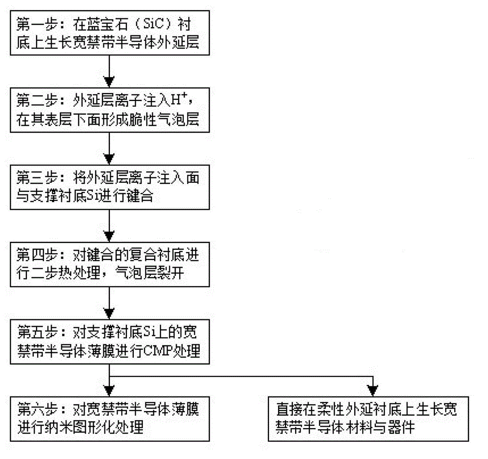
[0032] A method for preparing a large-scale SiC homoepitaxial flexible substrate such as Figure 1 to Figure 6 As shown, the thickness of the SiC flexible functional layer is 20~50nm. The LED device with vertical structure can be prepared on the flexible substrate, which not only saves the cost, but also improves the light-emitting area and performance of the device.

[0033] Concrete preparation steps are as follows:

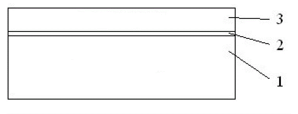
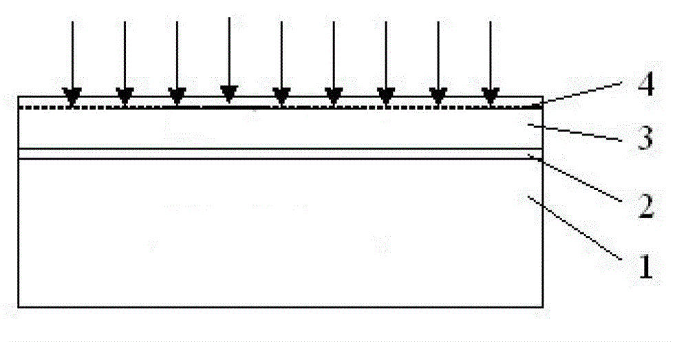
[0034] 1) The SiC epitaxial layer 3 is grown on the SiC or Si substrate 1 by high-temperature MOCVD, MBE and other technologies. There is a buffer layer 2 between the SiC epitaxial layer 3 and the SiC or Si substrate 1. The size of the SiC or Si substrate 1 is 2~6inch. A SiC thick film with low micropipe density is prepared by step-controlled epitaxy or position-competitive epitaxy, and the thickness of the thick film ranges from 5 μm to 10 mm.

[0035] 2) Perform H on the upper surface of SiC epitaxial layer 3 + implanted to form a brittle bubble layer 4 i...

Embodiment 2

[0040] A method for preparing a large-scale patterned GaN homoepitaxial flexible substrate such as Figure 1 to Figure 7 As shown, the thickness of the GaN flexible functional layer is 20~50nm. The LED device with vertical structure can be prepared on the flexible substrate, which not only saves the cost, but also improves the light-emitting area and performance of the device.

[0041] Concrete preparation steps are as follows:

[0042] 1) GaN epitaxial layer 3 is grown on sapphire or SiC substrate 1 by MOCVD, MBE or HVPE technology, and there is a buffer layer or superlattice 2 between GaN epitaxial layer 3 and sapphire or SiC substrate 1, SiC or Si substrate The size of 1 is 2~8inch. Using the most advanced MOCVD, MBE or HVPE technology, including buffer layer technology, superlattice technology, ELOG technology, etc. to prepare a dislocation density of 10 5 ~10 6 cm -2 GaN thick film, the thickness of the thick film ranges from 5μm to 10mm.

[0043] 2) Perform H on th...


PUM

PropertyMeasurementUnit
Thicknessaaaaaaaaaa
Thicknessaaaaaaaaaa

Abstract

The invention discloses a preparation method of a wide-forbidden-band semiconductor flexible substrate, in particular to a preparation method of a GaN, AlN and SiC monocrystal flexible substrate, belonging to the technical field of microelectronics. The theory of the flexible substrate is introduced into the preparation process of a wide-forbidden-band semiconductor homoepitaxial substrate, the flexible substrate consists of a wide-forbidden-band semiconductor flexible function layer and a supporting substrate, and the thickness of the flexible function layer is 20-50nm. By using the flexible substrate, the defect density and the stress level of epitaxial materials are reduced and the crystal quality of the epitaxial materials is greatly improved; and the wide-forbidden-band semiconductor flexible substrate prepared by adopting the method has the advantages of large size and easiness in industrialization.

Description

technical field [0001] The invention belongs to the technical field of microelectronics, and in particular relates to a method for preparing a wide-bandgap semiconductor flexible substrate, in particular to a method for preparing a single-crystal GaN, AlN, and SiC flexible substrate. Background technique [0002] Wide bandgap semiconductors mainly include binary InN, GaN, AlN, SiC, ternary InGaN, AlGaN and quaternary InGaAlN and other materials, aluminum nitride (AlN), silicon carbide (SiC), gallium nitride (GaN) Base semiconductor materials are typical representatives of wide bandgap semiconductor materials. These materials have the characteristics of wide band gap, high thermal conductivity, high breakdown field strength, high saturation electron drift rate, small dielectric constant, high thermal conductivity, high radiation resistance, etc. It is an ideal material for high-temperature, radiation-resistant electronic devices, and has broad application prospects in nation...

Claims


Application Information

Patent Timeline
IPC IPC(8): H01L21/20H01L21/683
CPCH01L21/76254
Inventor 陈峰武魏唯韩云鑫巩小亮
Owner HUNAN RED SUN PHOTOELECTRICITY SCI & TECH
Why Eureka
Try Eureka