Manufacture method of isolation type power transistor

A technology of power transistors and manufacturing methods, applied in semiconductor/solid-state device manufacturing, electrical components, circuits, etc., can solve problems affecting chip performance, etc., and achieve the effects of low saturation voltage drop, reduced manufacturing cost, and high current drive capability

Active Publication Date: 2014-12-10
SHANGHAI HUAHONG GRACE SEMICON MFG CORP
View PDF4 Cites 0 Cited by
  • Summary
  • Abstract
  • Description
  • Claims
  • Application Information

AI Technical Summary

Problems solved by technology

However, with the increase of device density, the distance between transistors in chip cells is getting smaller and smaller, and the crosstalk between adjacent devices may affect each other, thereby affecting chip performance.

Method used


Image

  • Manufacture method of isolation type power transistor
  • Manufacture method of isolation type power transistor
  • Manufacture method of isolation type power transistor

Examples


Embodiment 1

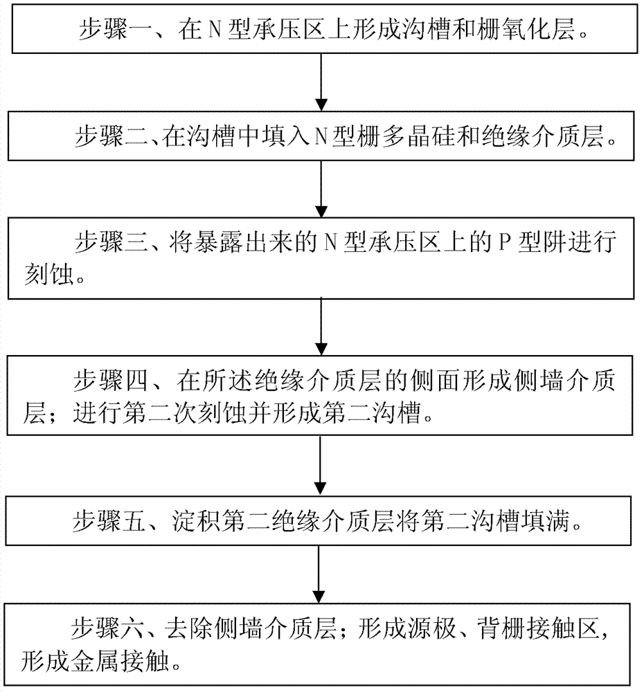
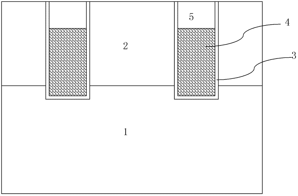
[0036] Such as figure 1 Shown is a flow chart of a method of the embodiment of the present invention; as Figure 2 to Figure 7C Shown is a schematic diagram of the device structure in each step of the method of Embodiment 1 of the present invention. Embodiment 1 of the present invention Manufacturing method of an isolated power transistor The gate of the isolated power transistor prepared has a trench structure, and the method of Embodiment 1 of the present invention includes the following steps:

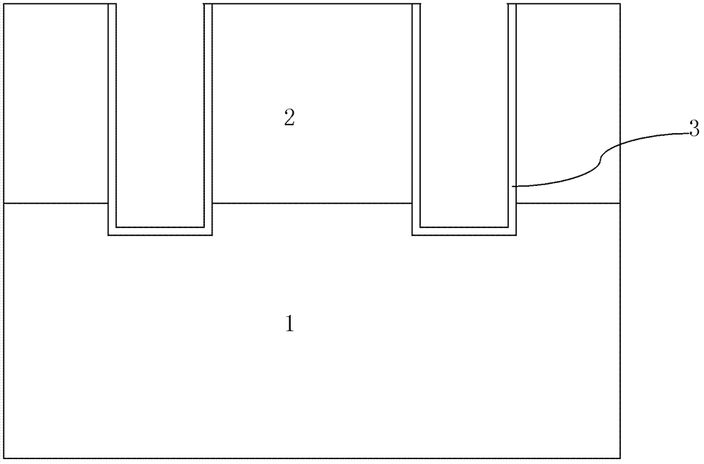
[0037] Step 1, such as figure 2 As shown, a trench is formed on the N-type pressure-bearing region 1 with a P-type well 2 formed on the top, the groove passes through the P-type well 2 and enters into the N-type pressure-bearing region 1, in the The bottom and sidewall surfaces of the trench form gate oxide layer 3 .

[0038] The isolated power transistor can be a silicon-based device or a compound semiconductor device. When the isolated power transistor is a silicon-based devi...

Embodiment 2

[0049] Such as Figure 8 Shown is the flow chart of the second method of the present invention; as Figure 9 to Figure 13B Shown is a schematic diagram of the device structure in each step of the method of Embodiment 2 of the present invention. The method for manufacturing an isolated power transistor according to Embodiment 2 of the present invention. The gate of the isolated power transistor prepared has a surface-type structure. The method according to Embodiment 2 of the present invention includes the following steps:

[0050] Step 1, such as Figure 9 As shown, a gate oxide layer 103, a gate polysilicon 104 and an insulating dielectric layer 105 are sequentially formed on the surface of the N-type pressure receiving region 101 from bottom to top; the insulating dielectric layer 105 and the gate polysilicon 104 are etched Etching is performed to form the gate, that is, the gate is composed of the etched gate polysilicon 104 .

[0051] The isolated power transistor can b...


PUM


Abstract

The invention discloses a manufacture method of an isolation type power transistor. By the manufacture method, insulating medium layers formed on the top of gate polycrystalline silicon and spacer medium layers formed on the side faces of the insulating medium layers serve as hard masks for etching to form isolation layer trenches among devices, and an insulated isolation layer can be formed among transistors without adding extra masks, so that density of the transistors in a chip cannot be decreased, and mutual interference of the devices can be weakened. Increase of the size of the transistors and increase of density of transistors in the chip are benefited, and powder devices lower in breakover resistance and saturation voltage drop and higher in current driving capacity can be obtained. Manufacture cost can be further reduced as adding of extra masks is not needed.

Description

technical field [0001] The invention relates to a manufacturing process method of a semiconductor integrated circuit, in particular to a manufacturing method of an isolated power transistor. Background technique [0002] In the application of power and high-voltage devices, it is hoped that the on-resistance of the transistor will be smaller, the saturation voltage drop will be lower, and the current driving capability will be greater. How to integrate more devices within a certain chip area is particularly important. However, with the increase of device density, the distance between transistors in chip cells is getting smaller and smaller, and the crosstalk between adjacent devices may affect each other, thereby affecting chip performance. Contents of the invention [0003] The technical problem to be solved by the present invention is to provide a method for manufacturing isolated power transistors, which can form an insulating isolation layer between transistors without...

Claims


Application Information

Patent Timeline
Patent Type & Authority Patents(China)
IPC IPC(8): H01L21/336H01L21/331
Inventor 韩峰段文婷
Owner SHANGHAI HUAHONG GRACE SEMICON MFG CORP
Why Eureka
Try Eureka