Method for determining etching time of sacrificial layer in real time

A technology of sacrificial layer and time, applied in the direction of coating, metal material coating process, and process for producing decorative surface effects, etc., can solve the problems of destroying chips, reducing yield, increasing tape-out time, etc., to improve reliability The effects of reliability, high yield, and reduced uncertainty

Inactive Publication Date: 2013-03-13
PEKING UNIV
View PDF5 Cites 6 Cited by
  • Summary
  • Abstract
  • Description
  • Claims
  • Application Information

AI Technical Summary

Problems solved by technology

This method will destroy certain chips, reduce the yield rate, and increase the tape-out time. It is not suitable for MEMS assembly line processing.

Method used


Image

  • Method for determining etching time of sacrificial layer in real time
  • Method for determining etching time of sacrificial layer in real time
  • Method for determining etching time of sacrificial layer in real time

Examples


Embodiment Construction

[0031] The present invention will be described in detail below through specific embodiments and accompanying drawings.

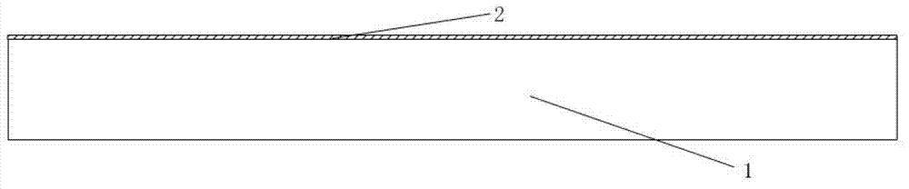
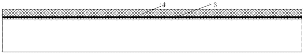
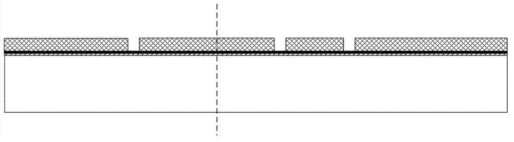
[0032] The corrosion time detection method of the present invention is mainly applicable to MEMS device chips with movable structures processed by surface sacrificial layer integration technology, such as sensors such as accelerometers and gyroscopes, and actuators such as adjustable capacitance structures. Taking the manufacture of a comb-shaped resonator as an example, the manufacture of the corrosion time detection structure and the manufacture of the resonator are combined. The specific process flow is shown in Figure 1, where the left side of the dotted line is the detection structure area, and the right side is the chip main structure area. , which is described as follows:

[0033] 1. Preparation: monocrystalline silicon substrate as the substrate of the chip;

[0034] 2. Deposit the substrate protective layer, including: LPCVD SiO2, with a thickness ...


PUM

PropertyMeasurementUnit
thicknessaaaaaaaaaa

Abstract

The invention relates to a method for determining etching time of a sacrificial layer in real time. The method comprises the following steps of: manufacturing the sacrificial layer and a structural layer of an MEMS (Micro Electro Mechanical System) device on a substrate by virtue of a surface sacrificial layer process; depositing a metal layer on the structural layer; and carrying out wet etching on the sacrificial layer, and determining finish time of etching by observing the dropping condition of metal in the metal layer. By virtue of the method, the etching time of the sacrificial layer can be determined in non-contact and non-destructive manners through naked-eye observation, and the process quality and the rate of finished products of the MEMS can be improved.

Description

technical field [0001] The invention belongs to the field of micro-electromechanical system (MEMS) processing technology, is particularly applied in the field of MEMS surface sacrificial layer technology, and relates to a method for determining the wet etching time of the MEMS surface sacrificial layer technology. The corrosion time is determined in real time through a test structure. Background technique [0002] Since the 1990s, microelectromechanical systems (MEMS) technology has entered a stage of rapid development, not only because of the novel concept, but also because MEMS devices have the characteristics of miniaturization, integration and better performance compared with traditional devices. Now MEMS has been widely used in automobiles, aerospace, information control, medicine, biology and other fields. MEMS technology is mainly divided into three categories: bulk silicon technology, surface sacrificial layer technology, and some special MEMS processing technology. ...

Claims


Application Information

Patent Timeline
Patent Type & Authority Applications(China)
IPC IPC(8): B81C1/00
Inventor 赵丹淇张大成何军黄贤杨芳田大宇刘鹏王玮李婷罗葵
Owner PEKING UNIV
Why Eureka
Try Eureka