Low-consumption low-minor lobe high-gain planar frequency scan antenna

A frequency scanning antenna, low side lobe technology, applied in the direction of antenna, antenna coupling, antenna array, etc., can solve the problems of different distribution of arrays, large transmission loss, large fluctuation of frequency band gain, etc., and achieve amplitude distribution control. Convenient and easy-to-implement effects with high design flexibility

Inactive Publication Date: 2013-03-20
NANJING UNIV OF SCI & TECH
View PDF3 Cites 13 Cited by
  • Summary
  • Abstract
  • Description
  • Claims
  • Application Information

AI Technical Summary

Problems solved by technology

However, due to the requirements of planarized circuits, these leaky-wave antennas for frequency scanning have a common problem, that is, the loss
Due to the planar printing process, the introduction of dielectric loss makes the transmission loss of the planar leaky wave antenna much larger than that of the waveguide frequency-sweep antenna, which cannot achieve high-gain frequency-sweep array antennas, and often has large gain fluctuations in the frequency band.
In addition, since the traveling wave t

Method used


Image

  • Low-consumption low-minor lobe high-gain planar frequency scan antenna
  • Low-consumption low-minor lobe high-gain planar frequency scan antenna
  • Low-consumption low-minor lobe high-gain planar frequency scan antenna

Examples


Embodiment 1

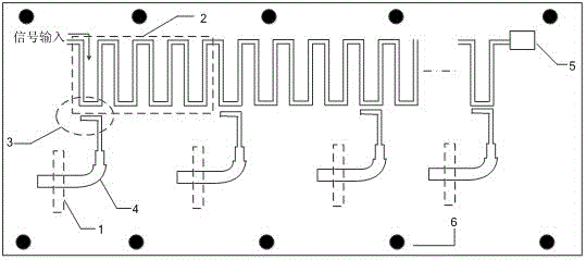
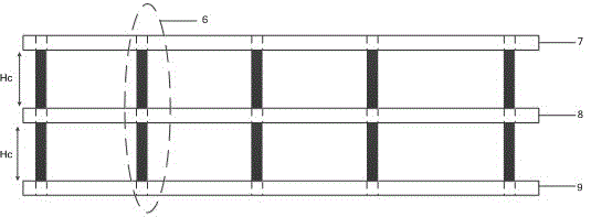
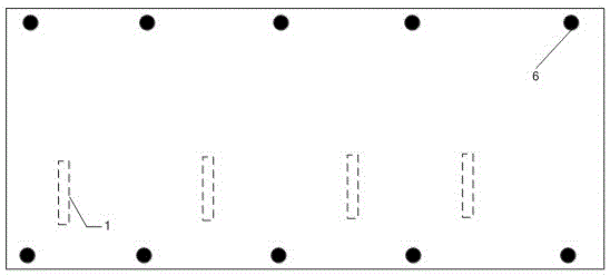
[0029] A low-consumption, low-sidelobe, high-gain planar frequency scanning antenna is composed of three planar dielectric substrates, the three planar dielectric substrates are arranged overlappingly, and there is an interval between each planar dielectric substrate, and the three planar dielectric substrates are passed through plastic screws 6 Fixed, wherein the first layer of planar dielectric substrate 7 includes the antenna radiation unit and the floor, and the upper and lower surfaces of the second layer of planar dielectric substrate 8 are symmetrically arranged, including a slow wave serpentine line structure 2, a coupling power divider 3, and a transmission line feed structure 4. Matching load 5, the end of the slow-wave serpentine line structure 2 is connected to the matching load 5, the slow-wave serpentine line structure 2 is coupled and connected to the coupling power divider 3, and the transmission line feed structure 4 is connected to the coupling power divider 3,...

Embodiment 2

[0039] It consists of three layers of planar dielectric substrates, the three layers of planar dielectric substrates are arranged overlappingly, and there is an interval between each layer of planar dielectric substrates, and the three layers of planar dielectric substrates are fixed by plastic screws 6, wherein the first layer of planar dielectric substrates 7 includes antenna radiation The unit and the floor, the upper and lower surfaces of the second plane dielectric substrate 8 are symmetrically arranged, including the slow wave serpentine line structure 2, the coupling power divider 3, the transmission line feed structure 4, the matching load 5, and the slow wave serpentine line structure 2 The end is connected to the matching load 5, the slow wave serpentine line structure 2 is coupled and connected to the coupling power divider 3, the transmission line feed structure 4 is connected to the coupling power divider 3, and the third plane dielectric substrate 9 is the floor. ...

Embodiment 3

[0045] It consists of three layers of planar dielectric substrates, the three layers of planar dielectric substrates are arranged overlappingly, and there is an interval between each layer of planar dielectric substrates, and the three layers of planar dielectric substrates are fixed by plastic screws 6, wherein the first layer of planar dielectric substrates 7 includes antenna radiation The unit and the floor, the upper and lower surfaces of the second plane dielectric substrate 8 are symmetrically arranged, including the slow wave serpentine line structure 2, the coupling power divider 3, the transmission line feed structure 4, the matching load 5, and the slow wave serpentine line structure 2 The end is connected to the matching load 5, the slow-wave serpentine line structure 2 is coupled to the coupling power divider 3, the transmission line feed structure 4 is connected to the coupling power divider), and the third layer of planar dielectric substrate 9 is the floor.

[00...


PUM


Abstract

The invention discloses a low-consumption low-minor lobe high-gain planar frequency scan antenna, which comprises three layers of planar dielectric substrates that are overlapped, wherein gaps are formed among the three layers of planar dielectric substrates; the three layers of planar dielectric substrates are fixed by plastic screws; the first layer of planar dielectric substrate comprises an antenna radiating element and a floor; the upper surface and the lower surface of the second layer of planar dielectric substrate are symmetrically arranged; the second layer of planar dielectric substrate comprises a slow-wave serpentine curve structure, a power divider, a transmission line feed structure and a matched load; the terminal of the slow-wave serpentine curve structure is connected to the matched load; the slow-wave serpentine curve structure is connected with the power divider; the transmission line feed structure is connected with the power divider; and the third layer of planar dielectric substrate is a floor. The antenna is low in consumption, and minor lobe, high in gain, simple in structure and convenient to implement.

Description

technical field [0001] The invention belongs to the technical field of antennas, in particular to a plane frequency scanning antenna with low consumption, low side lobe and high gain. Background technique [0002] With the continuous development of modern radar technology, the requirements for antenna tracking speed are increasing day by day. The electronic scanning antenna has basically replaced the mechanical scanning antenna because of its extremely low wave velocity scanning time, small signal attenuation, and good operating performance. The principle of using frequency scanning to realize beam scanning is simple, the structure of the feeding network is simple, and the cost is relatively low. The traditional frequency scanning antenna consists of a serpentine slow-wave waveguide structure as a phase shifting unit and a waveguide slot antenna as a radiating unit. Due to the extremely low loss of the waveguide, frequency-sweeping antenna arrays of higher gain can be reali...

Claims


Application Information

Patent Timeline
IPC IPC(8): H01Q1/52H01Q3/34H01Q21/00H01Q1/38H01Q1/48
Inventor 吴文崔兰方大纲
Owner NANJING UNIV OF SCI & TECH
Why Eureka
Try Eureka