
Low source-drain contact resistance mosfets and manufacturing method thereof

A source-drain contact and resistance technology, used in semiconductor/solid-state device manufacturing, circuits, electrical components, etc., can solve problems such as difficulty in adoption, reduce source-drain contact resistance, and increase process complexity, and achieve reduced height and source-drain. Contact resistance, the effect of improving performance

Active Publication Date: 2015-11-25
INST OF MICROELECTRONICS CHINESE ACAD OF SCI
View PDF5 Cites 0 Cited by
  • Summary
  • Abstract
  • Description
  • Claims
  • Application Information

AI Technical Summary

Problems solved by technology

[0016] However, the above three methods have significant limitations
[0017] For the above method 1, due to the limitation of the solid solubility limit of dopants or impurities in silicon, it is impossible to continuously increase the doping concentration N of the source and drain regions, that is, there is a maximum value of N
[0018] For the above method 2, due to the different materials of silicide, it is necessary to make different layouts and deposit different metal materials according to the different types of N and PMOS when making MOS, which greatly increases the complexity of the process and cannot be applied to actual production.
[0019] For the above method 3, only changing the material of the source and drain regions seems to be a relatively simple process, but the doping concentration of impurities in Si1-xGex is not as high as that in Si, that is, although m* is reduced, N is also reduced, The ρc reduction effect of the whole device is not obvious
[0020] It can be seen that in the existing manufacturing technology of doped source-drain MOSFETs, it is difficult to use known methods to effectively reduce the source-drain contact resistance

Method used


Image

  • Low source-drain contact resistance mosfets and manufacturing method thereof
  • Low source-drain contact resistance mosfets and manufacturing method thereof
  • Low source-drain contact resistance mosfets and manufacturing method thereof

Examples


Embodiment Construction

[0042] The features and technical effects of the technical solution of the present invention will be described in detail below with reference to the accompanying drawings and in conjunction with exemplary embodiments, and a semiconductor device capable of effectively reducing source-drain contact resistance and a manufacturing method thereof are disclosed. It should be pointed out that similar reference numerals represent similar structures, and the terms "first", "second", "upper", "lower" and the like used in this application can be used to modify various device structures or manufacturing processes . These modifications do not imply spatial, sequential or hierarchical relationships of the modified device structures or fabrication processes unless specifically stated.

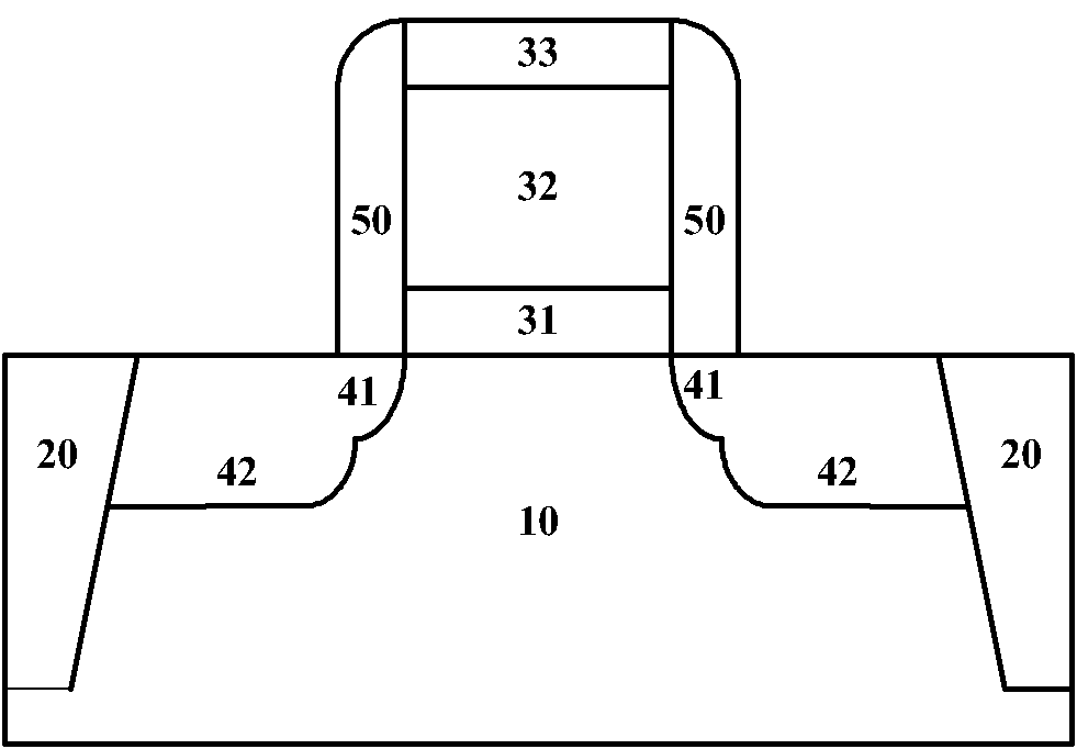
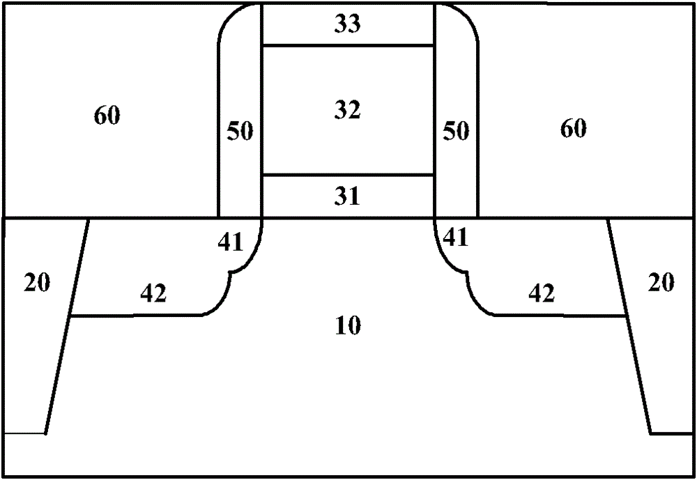
[0043] Figure 2 to Figure 10 It is a schematic cross-sectional view of various steps of a semiconductor device capable of effectively reducing source-drain contact resistance and a manufacturing method ther...


PUM


Abstract

The invention discloses a MOSFET (metal-oxide-semiconductor field effect transistor) which effectively lowers source-drain contact resistance in post grid process and a manufacturing method thereof. The MOSFET comprises a substrate, a grid stacking structure, formed by a grid medium layer and a grid metal layer, on the substrate, source-drain areas in substrate parts on two sides of the grid stacking structure, grid side walls on substrate parts on two sides of the grid stacking structure, interlevel dielectric on the substrate, a source-drain contact plug in the interlevel dielectric on the source-drain areas and metal silicide between the source-drain areas and the source-drain contact plug and is characterized in that the interface of the metal silicide and the source-drain areas is provided with an ion-doped dephlegmation area, and the grid medium layer is located below and on the side of the grid metal layer. By the MOSFET which effectively lowers source-drain contact resistance and the manufacturing method thereof and the ion-doped dephlegmation area disposed on the interface between the metal silicide and the source-drain areas, Schottky barrier height can be reduced effectively, and accordingly source-drain resistance is reduced greatly, and device performance is further improved.

Description

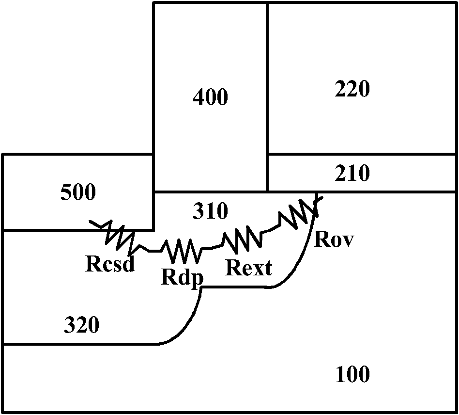
technical field [0001] The invention relates to a semiconductor device and a manufacturing method thereof, in particular to a MOSFETS manufactured by a gate-last process that effectively reduces the source-drain contact resistance and a corresponding manufacturing method thereof. Background technique [0002] The continuous increase of IC integration requires the continuous reduction of device size, but the electrical operating voltage sometimes remains unchanged, which makes the electric field strength in the actual MOS device continue to increase. The high electric field brings a series of reliability problems, which degrades the performance of the device. For example, parasitic series resistance between the source and drain regions of a MOSFET will cause the equivalent operating voltage to drop. [0003] figure 1 Shown is a MOSFET with metal silicide on the heavily doped source and drain in the prior art, wherein a gate stack structure 200 composed of a gate dielectric ...

Claims


Application Information

Patent Timeline
Patent Type & Authority Patents(China)
IPC IPC(8): H01L29/49H01L29/78H01L21/28H01L21/336
Inventor 罗军赵超叶甜春
Owner INST OF MICROELECTRONICS CHINESE ACAD OF SCI
Learn More