Fast recovery diode and manufacturing method thereof

A fast recovery, diode technology, applied in semiconductor/solid-state device manufacturing, electrical components, circuits, etc., can solve the problems of limited improvement and high manufacturing cost, and achieve the effects of reducing vibration, improving safe working area, and avoiding surface leakage

Active Publication Date: 2013-04-03
GLOBAL ENERGY INTERCONNECTION RES INST CO LTD +1
View PDF6 Cites 11 Cited by
  • Summary
  • Abstract
  • Description
  • Claims
  • Application Information

AI Technical Summary

Problems solved by technology

However, the improvement of this method is limited, because when the concentration of the P-type doped region is reduced too much, the contact resistance with the anode metal will increase, and the depletion region is close to the silicon surface during reverse bias, and the reverse leakage current will increase; the patent number is 97112472.8 ( image 3 ) adopts the P+ / P (222 / 221) two-layer structure, although it is beneficial to the dynamic performance of FRD, but a photolithography process is added, and the manufacturing cost is relatively high

Method used


Image

  • Fast recovery diode and manufacturing method thereof
  • Fast recovery diode and manufacturing method thereof
  • Fast recovery diode and manufacturing method thereof

Examples


Embodiment 1

[0033] Embodiment 1 The manufacturing method of the fast recovery diode of the present invention

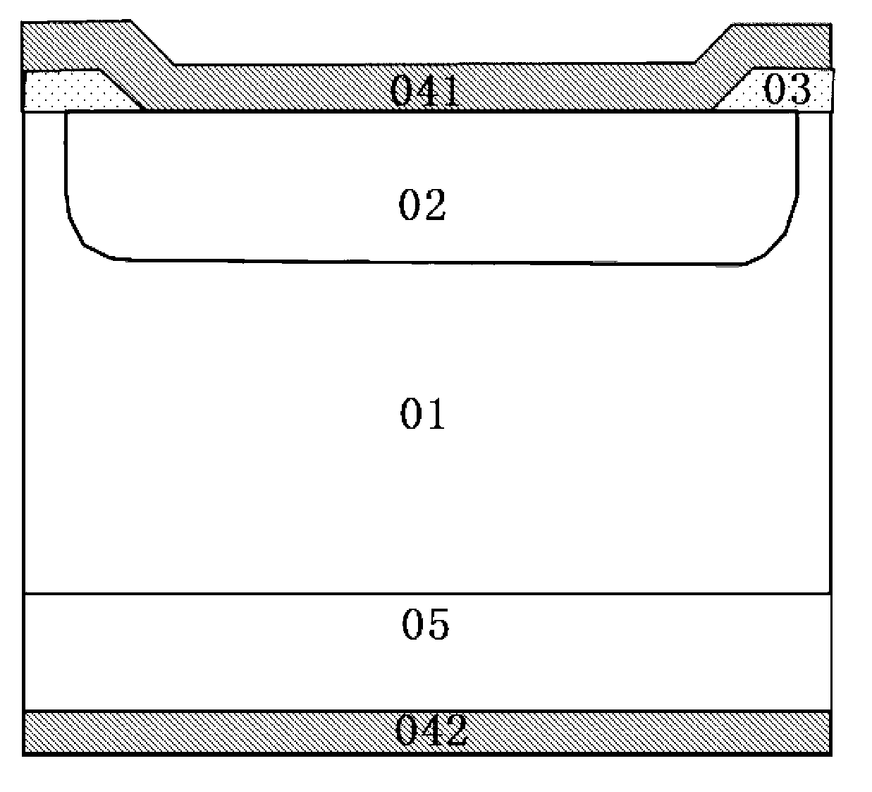
[0034] 1) Field oxidation: After cleaning the uniformly doped N-type silicon substrate 01, a high-temperature oxidation method is used to grow a 1-4um oxide layer 03 on the surface of the silicon wafer, such as: Figure 7 shown. N-type silicon substrate 01 can be prepared by using epitaxial wafer or single wafer. Considering the current technology level and cost control, the former is more suitable for medium and low voltage products, and the latter is more suitable for the development of medium and high voltage devices;

[0035] 2) Doping window etching: After the processes of gluing, exposing, developing, oxide layer etching and degumming, the P-type doped ion implantation window D is photolithographically obtained, such as Figure 8 shown;

[0036] 3) Doping of the emitter region: the oxide layer 03 is used as an implantation masking window, and P-type impurities are implant...

Embodiment 2

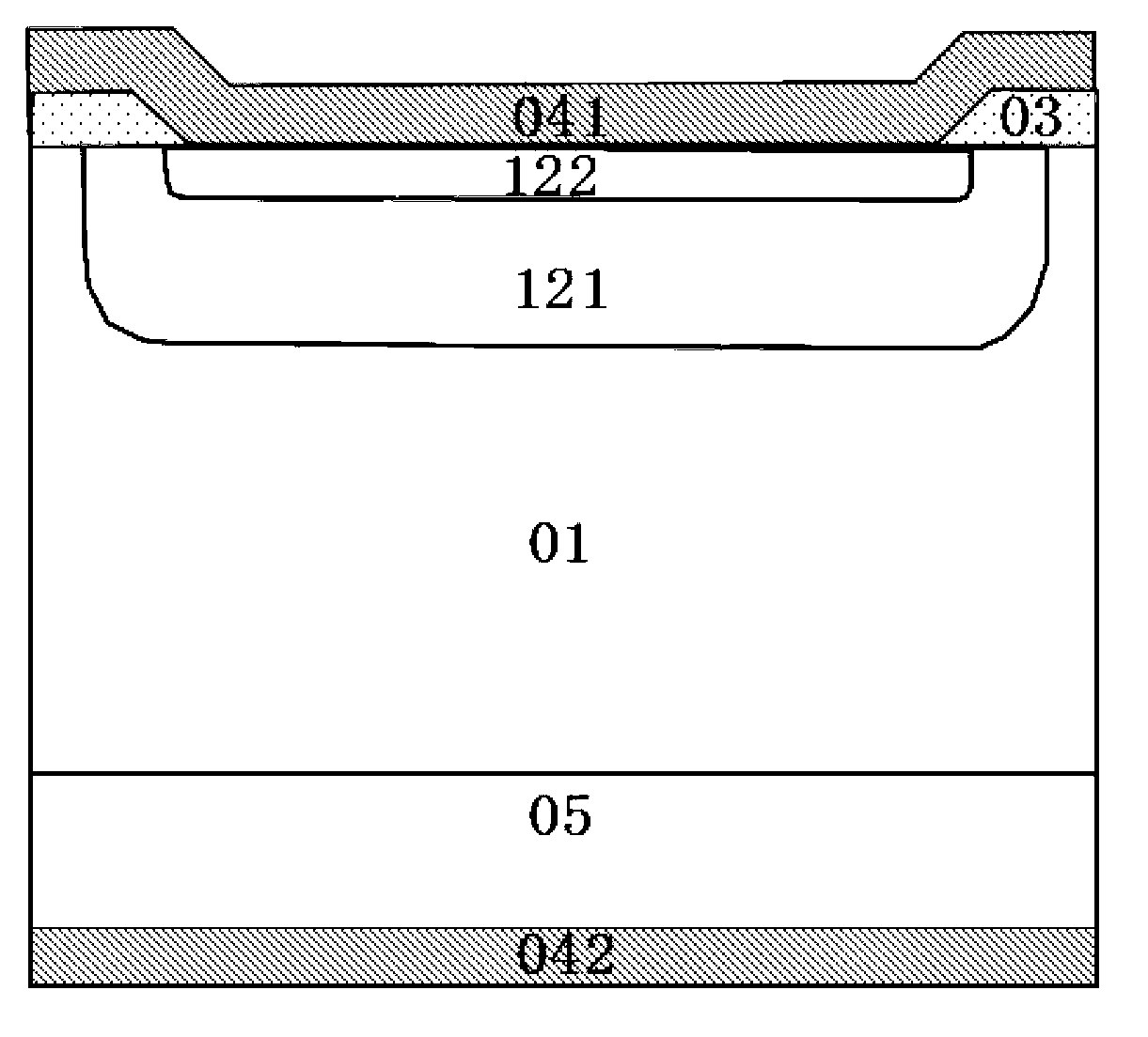
[0042] In the emission region, the overlapping P-type regions 322 in a wave shape are realized by means of local implantation of P-type ions 321 and high-temperature push junctions. The top view shape of the implantation window of the P-type ion 321 can be diversified, such as regular hexagon, square, circle and interdigital shape, etc., such as Figure 4 shown.

Embodiment 3

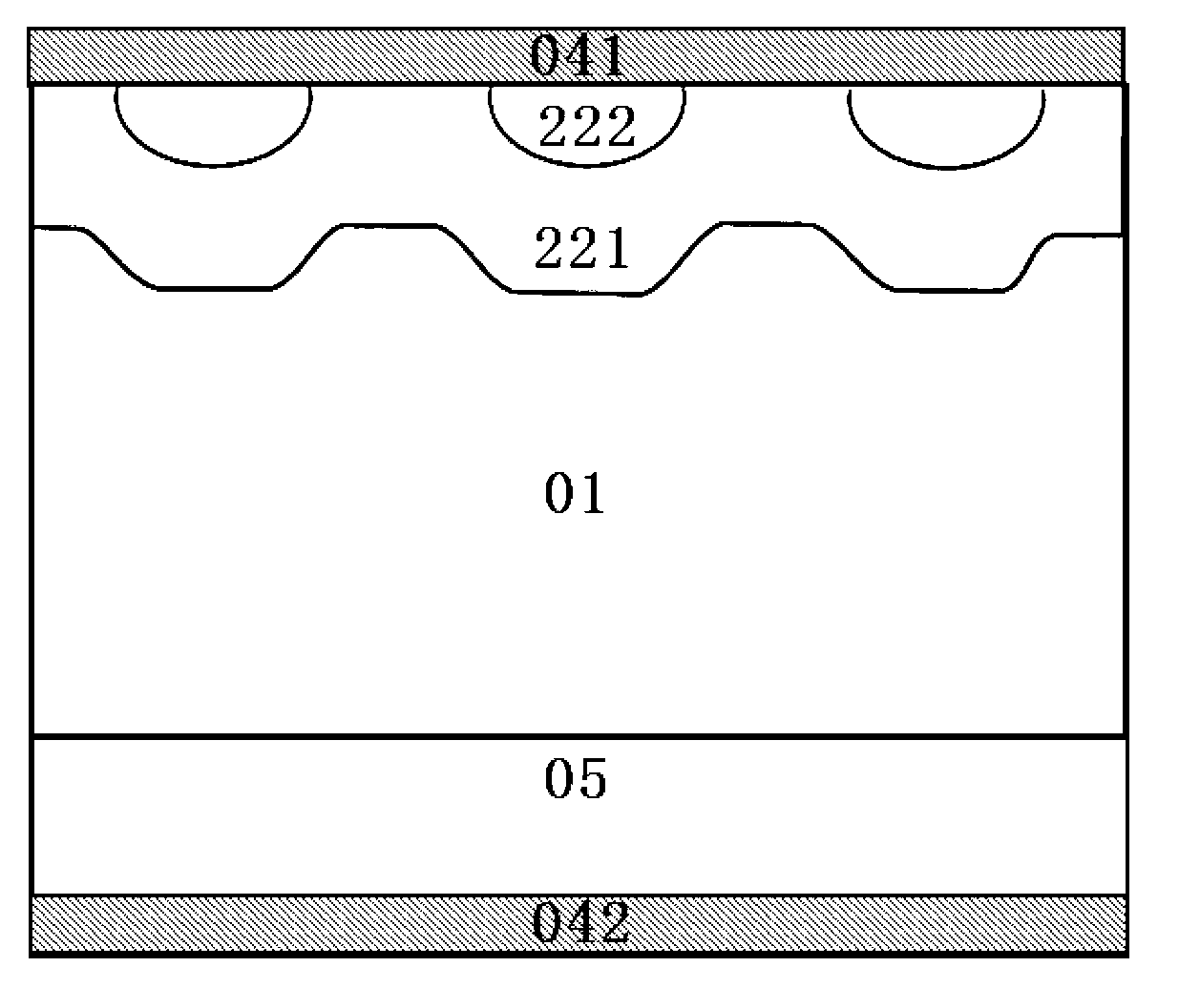
[0044] The implantation windows 321 of P-type ions are equally spaced, and the ion implantation windows are regular hexagons, such as Figure 5 shown.

[0045] After implantation through the regular hexagonal implantation window, a wavy P-type doping structure with high (highly doped P region HP) and low concentration (lowly doped P region LP) is formed, such as Image 6 322 shown.


PUM


Abstract

The invention discloses a fast recovery diode and a manufacturing method of the fast recovery diode. The diode disclosed by the invention comprises an anodic diffusion P-type doped region, an evenly-doped intrinsic region, a cathodic diffusion N-type region, anode and cathode metal layers, wherein the anodic diffusion P-type doped region is a P-type doped region provided with alternated high and low concentrations and formed by locally pouring through a mask plate. Compared with the prior art, the diode disclosed by the invention has the characteristics of low inverse peak current IRRM, short reverse recovery time trr and high reverse recovery softness.

Description

【Technical field】 [0001] The invention relates to a semiconductor power device, in particular to a fast recovery diode and a manufacturing method. 【Background technique】 [0002] Fast recovery diodes (FRDs) are widely used in medium and low voltage, high voltage and ultra-high voltage fields. With the development of high-end markets such as power systems and locomotive traction, higher and higher requirements are placed on the working characteristics and reliability of FRDs. [0003] like figure 1 The conventional FRD shown is a PIN three-layer structure. During forward conduction, holes in the P-type doping region 02 and electrons in the N-type doping region 05 are injected into the intrinsic region 01 respectively and recombine in this region to form conductance modulation. However, the more carriers are stored in the intrinsic region 01, the lower the on-resistance and the lower the forward voltage drop VF. If a reverse bias voltage is applied to the FRD at this time, ...

Claims


Application Information

Patent Timeline
Patent Type & Authority Applications(China)
IPC IPC(8): H01L29/861H01L29/06H01L21/329
Inventor 刘钺杨高文玉王耀华张冲金锐于坤山
Owner GLOBAL ENERGY INTERCONNECTION RES INST CO LTD
Why Eureka
Try Eureka