Groove MOS (metal oxide semiconductor) structure Schottky diode and preparation method thereof

A technology of Schottky diode and MOS structure, which is applied in semiconductor/solid-state device manufacturing, electrical components, circuits, etc., can solve the problems that cannot be applied in high-voltage environment, fast turn-on and turn-off speed, low forward turn-on voltage, etc., to achieve The effect of compact product structure, reduced production cycle, and reduced process requirements

Active Publication Date: 2013-04-03
ZHEJIANG UNIV
View PDF3 Cites 6 Cited by
  • Summary
  • Abstract
  • Description
  • Claims
  • Application Information

AI Technical Summary

Problems solved by technology

[0002] Power semiconductor devices are widely used in power management and power applications, especially semiconductor devices with trench structures have become an important trend in device development. S...

Method used


Image

  • Groove MOS (metal oxide semiconductor) structure Schottky diode and preparation method thereof
  • Groove MOS (metal oxide semiconductor) structure Schottky diode and preparation method thereof
  • Groove MOS (metal oxide semiconductor) structure Schottky diode and preparation method thereof

Examples


Embodiment 1

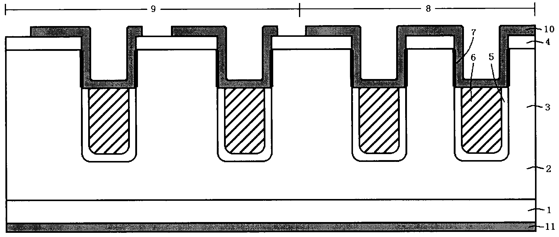
[0027] figure 1 Be a kind of trench MOS structure Schottky diode of the present invention, combine below figure 1 The semiconductor device of the present invention will be described in detail.

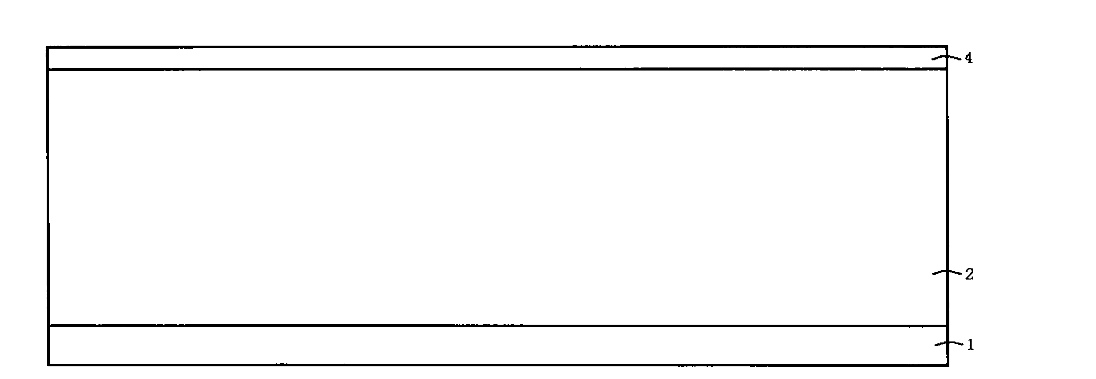
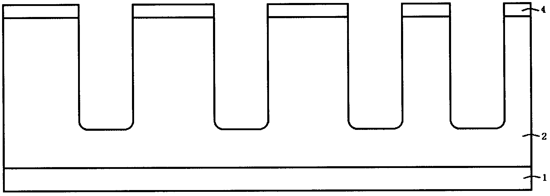
[0028] A Schottky diode with a trench MOS structure, comprising: a substrate layer 1, which is an N-conductive semiconductor silicon material, on the lower surface of the substrate layer 1, an electrode is drawn out through a metal layer 11 on the lower surface; a drift layer 2, located on the substrate layer 1 The upper part is a semiconductor silicon material of N conductivity type; the drift layer trench region 3 is located on the upper part of the drift layer 2; the thermal oxidation layer 4 is located on the upper surface of the drift layer 2 and is an oxide of semiconductor silicon material; the vertical trench is located in the silicon body, A gate oxide layer 5 is grown on its inner wall, the trench is filled with gate polysilicon 6, and there is a Schottky barrier junction 7 ...


PUM


Abstract

The invention discloses a groove MOS (metal oxide semiconductor) structure Schottky diode. The electric field intensity distribution of a drifting region is changed through an MOS structure, so that a peak value electric field appears in a semiconductor material close to the bottom part of a groove, and does not appear close to a Schottky barrier junction. The invention also provides a preparation method, so that devices can be produced and manufactured through photolithographic processes twice.

Description

technical field [0001] The invention relates to a trench MOS structure Schottky diode, and also relates to a preparation method of the trench MOS structure Schottky diode. Background technique [0002] Power semiconductor devices are widely used in power management and power supply applications. Especially semiconductor devices with trench structures have become an important trend in device development. Schottky devices have the advantages of low forward turn-on voltage and fast turn-on and turn-off speed. Schottky devices also have a large reverse leakage current and cannot be used in high-voltage environments. [0003] Schottky diodes can be fabricated by a number of different layout techniques, the most common being planar layout. A typical trench-type layout is shown in B J Baliga Patent No. 5,612,567. The fabrication process for trench Schottky diodes requires a large number of masks and fabrication steps. There is a need to fabricate trench Schottky diodes by improv...

Claims


Application Information

Patent Timeline
IPC IPC(8): H01L29/872H01L21/329
Inventor 朱江盛况
Owner ZHEJIANG UNIV
Why Eureka
Try Eureka