Reverse conducting insulated gate bipolar transistor (IGBT) semiconductor device and manufacture method thereof

A manufacturing method and semiconductor technology, applied in the manufacture of reverse conduction type IGBT semiconductor devices, in the field of reverse conduction type IGBT semiconductor devices, can solve the problems that cannot meet the needs of activation and diffusion of blocking layers, and the depth of laser activation is limited, etc., to achieve increased depth, improve activation efficiency, and achieve integrated effects

Active Publication Date: 2013-04-10
SHANGHAI HUAHONG GRACE SEMICON MFG CORP
View PDF6 Cites 27 Cited by
  • Summary
  • Abstract
  • Description
  • Claims
  • Application Information

AI Technical Summary

Problems solved by technology

However, the activation depth of the laser is limited, generally only 1-2 microns, which cannot meet the needs of activation and diffusion of 3-30 micron field-blocking layers

Method used


Image

  • Reverse conducting insulated gate bipolar transistor (IGBT) semiconductor device and manufacture method thereof
  • Reverse conducting insulated gate bipolar transistor (IGBT) semiconductor device and manufacture method thereof
  • Reverse conducting insulated gate bipolar transistor (IGBT) semiconductor device and manufacture method thereof

Examples


Embodiment 1

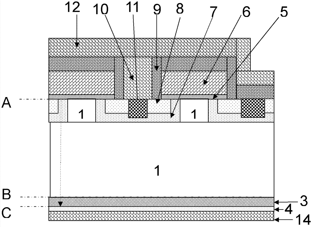
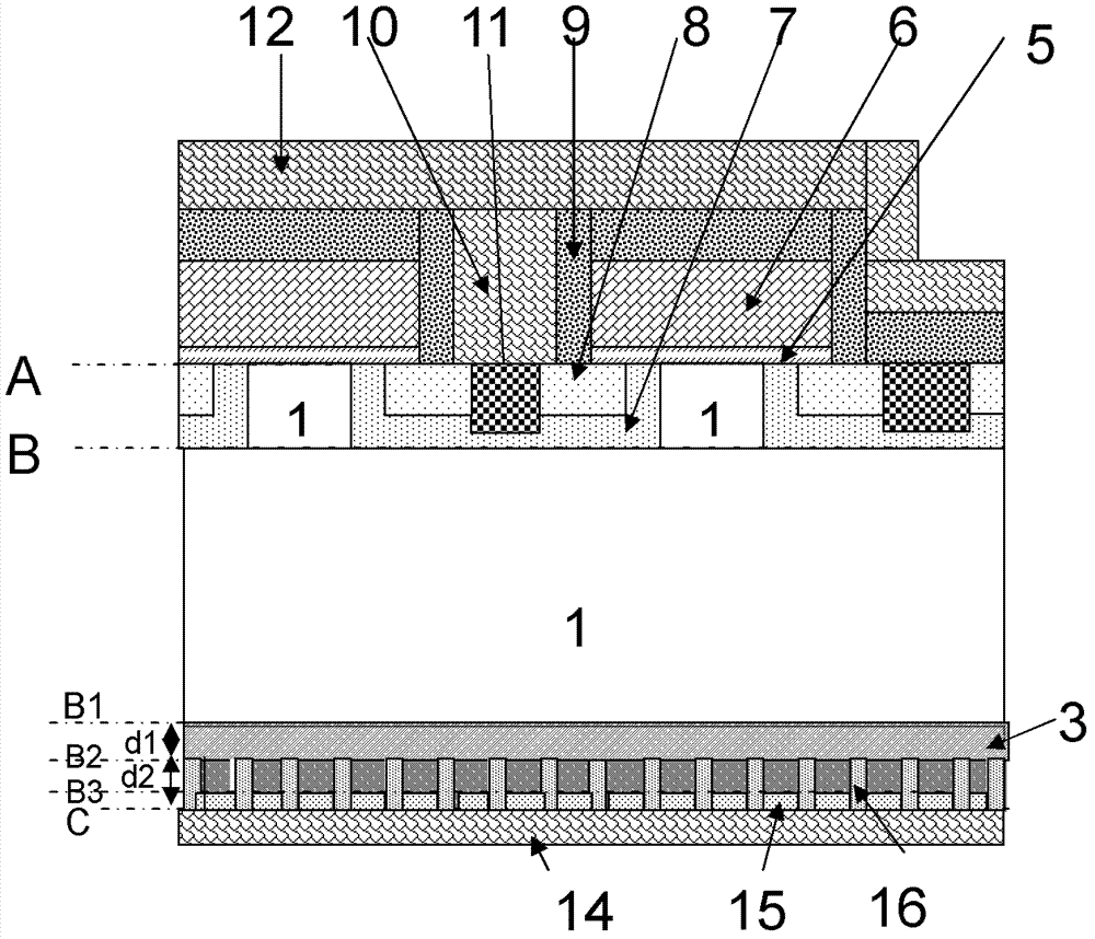
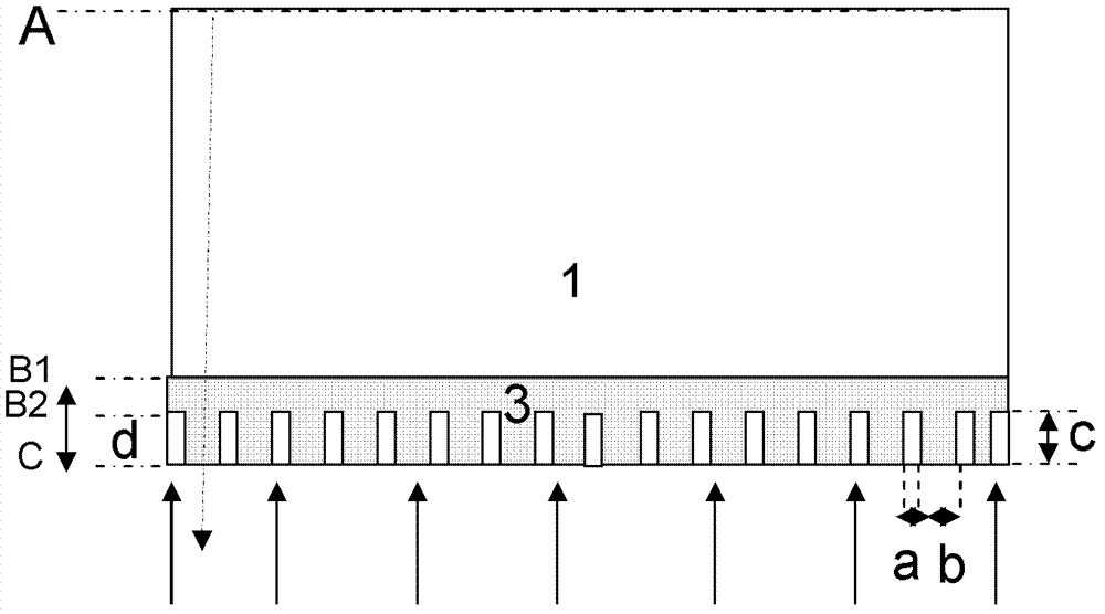
[0066] like Figure 3A to Figure 3D Shown is a device structure diagram in each step of a manufacturing method of a reverse conduction type IGBT semiconductor device according to an embodiment of the present invention. Embodiment 1 of the present invention is a method for manufacturing a reverse conduction type IGBT semiconductor device, comprising the following steps:

[0067] Step 1, such as Figure 3A As shown, first provide an impurity concentration C1 = 2.4E13CM -3 . An N-type silicon substrate 1 with a resistivity of 90 ohm.cm, and the thickness of the silicon substrate 1 is more than 700 microns. A first dielectric film is deposited on the front side of the silicon substrate 1 to protect the front side of the silicon substrate 1 well. The first dielectric film described in Embodiment 1 of the present invention is an oxide film with a thickness of 5000 angstroms to 20000 angstroms.

[0068] Thinning the N-type silicon wafer 1 from the back, and thinning the silicon w...


PUM


Abstract

The invention discloses a reverse conducting insulated gate bipolar transistor (IGBT) semiconductor device. A groove is formed on the rear side of a silicon substrate, the groove cuts a field blocking layer into a three-dimensional structure, and therefore the depth of the field blocking layer can be increased and activation efficiency of the field blocking layer is improved. A first electrode area provided with a fast recovery diode is formed in the groove, and therefore integration of the IGBT device and the fast recovery diode is achieved. The invention further discloses a manufacture method of the reverse conducting IGBT semiconductor device.

Description

technical field [0001] The invention relates to the field of manufacturing semiconductor integrated circuits, in particular to a reverse conduction type IGBT semiconductor device; the invention also relates to a method for manufacturing the reverse conduction type IGBT semiconductor device. Background technique [0002] Among high-voltage devices, insulated-gate bipolar transistors (IGBTs) have been used more and more widely in devices with voltages above 600 volts, and have recently been developed in the direction of high voltage and high current density. In the use of IGBTs, IGBTs are usually combined with fast recovery diodes (FAST RECOVERED DIODE, FRD) in a module package to reduce switching power consumption and provide reverse current conduction capabilities. Recently, some companies have begun to integrate FRD into IGBT chips to further increase the current density of the device, especially to reduce the difficulty of module packaging, improve the reliability of modul...

Claims


Application Information

Patent Timeline
Patent Type & Authority Applications(China)
IPC IPC(8): H01L29/739H01L21/331H01L21/265
CPCH01L29/66333H01L29/7395H01L29/861H01L29/0834H01L29/7393H01L29/06H01L21/265H01L29/66325
Inventor 肖胜安
Owner SHANGHAI HUAHONG GRACE SEMICON MFG CORP
Why Eureka
Try Eureka