Metallic oxide semiconductor film and preparation method and application thereof

An oxide semiconductor and oxide thin film technology, which is applied in the manufacture of semiconductor/solid-state devices, semiconductor devices, transistors, etc., can solve the problems of high annealing temperature, poor performance of thin-film semiconductors, and poor annealing efficiency, and achieve good stability, Strong performance stability, saving process time

Active Publication Date: 2013-04-24
CHENGDU VISTAR OPTEOLECTRONICS CO LTD
View PDF6 Cites 9 Cited by
  • Summary
  • Abstract
  • Description
  • Claims
  • Application Information

AI Technical Summary

Problems solved by technology

[0008] For this reason, the technical problem to be solved by the present invention is that in the prior art, metal oxide thin films formed based on ZnO and added with other metal elements have high annealing temperat

Method used


Image

  • Metallic oxide semiconductor film and preparation method and application thereof
  • Metallic oxide semiconductor film and preparation method and application thereof
  • Metallic oxide semiconductor film and preparation method and application thereof

Examples


Embodiment 1

[0053] The metal oxide semiconductor thin film described in this embodiment is an IGZO thin film, which is prepared by the following steps:

[0054] (1) Prepare the desired IGZO metal oxide film by radio frequency magnetron sputtering

[0055] The specific steps are: a certain proportion of Ar and O is introduced into the vacuum chamber. 2 The mixed gas, apply an electric field between the substrate IGZO targets, and use a high-density magnetic field to scan the IGZO targets. Ar ions hit the IGZO target under the action of an electric field, sputtering atoms or atomic groups of In, Ga, and Zn, and these atoms or atoms are deposited on the glass substrate to form a 30nm thick IGZO film;

[0056] (2) Laser annealing procedure

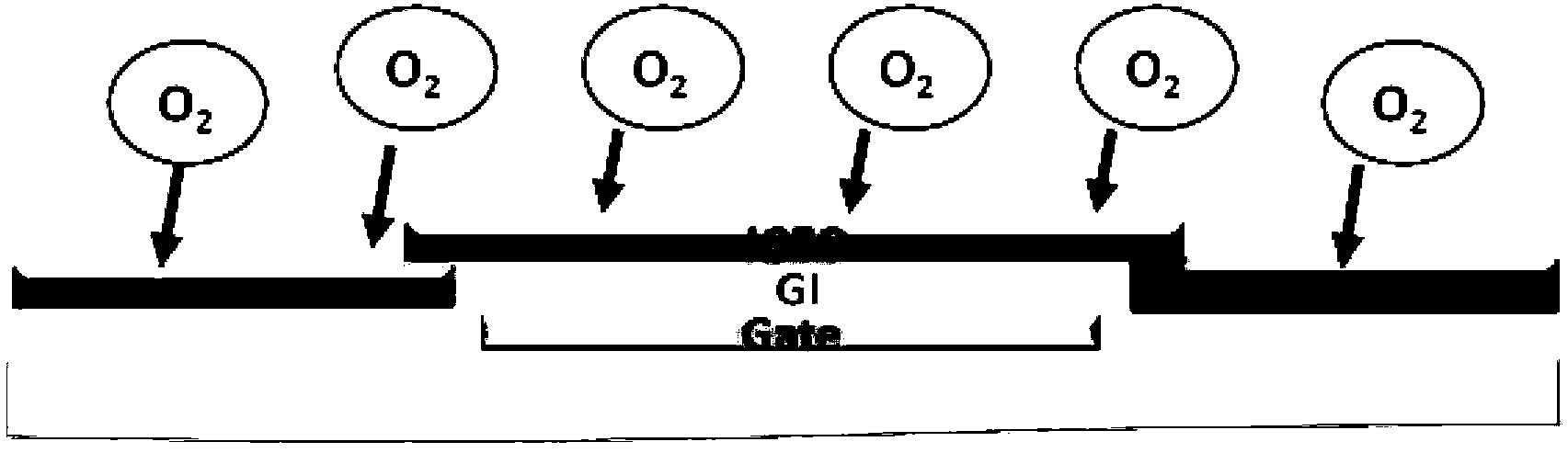
[0057] The specific steps are: a certain proportion of N is introduced into the airtight chamber 2 and O 2 The mixed gas, adjust the oxygen content in the airtight chamber to 63%, and place the above-mentioned glass substrate deposited with the IGZO m...

Embodiment 2

[0070] The metal oxide semiconductor thin film described in this embodiment is an IGZO thin film, which is prepared by the following steps:

[0071] (1) Prepare the desired IGZO metal oxide film by radio frequency magnetron sputtering

[0072] The specific steps are: a certain proportion of Ar and O is introduced into the vacuum chamber. 2 The mixed gas, apply an electric field between the substrate IGZO targets, and use a high-density magnetic field to scan the IGZO targets. Ar ions hit the IGZO target under the action of an electric field, sputtering atoms or atomic groups of In, Ga, and Zn, and these atoms or atoms are deposited on the glass substrate to form a 30nm thick IGZO film;

[0073] (2) Laser annealing procedure

[0074] The specific steps are: a certain proportion of N is introduced into the airtight chamber 2 and O 2 The mixed gas, adjust the oxygen content in the airtight chamber to 10%, and place the above-mentioned glass substrate deposited with the IGZO m...

Embodiment 3

[0077] The metal oxide semiconductor thin film described in this embodiment is an IGZO thin film, which is prepared by the following steps:

[0078] (1) Same as step (1) in Example 1;

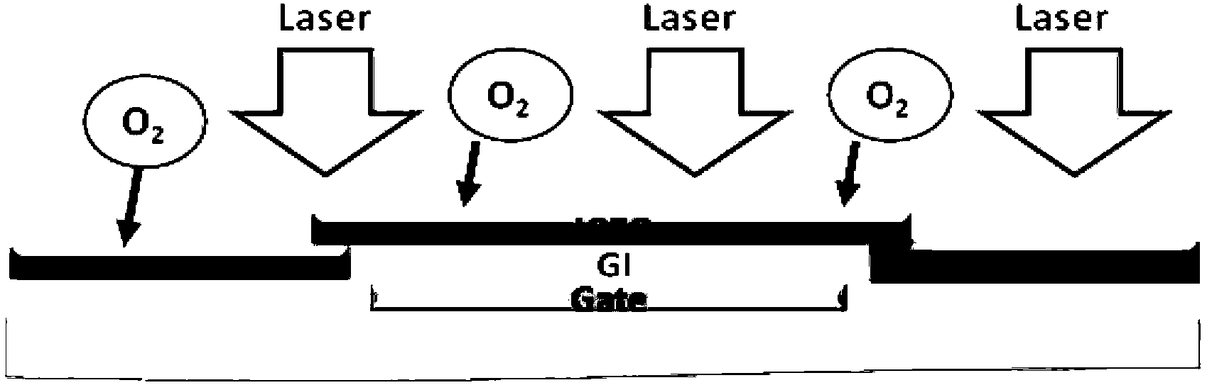
[0079] (2) Place the above-mentioned glass substrate deposited with IGZO metal oxide film on all O 2 In the closed chamber, the laser annealing is carried out by scanning the strip laser with a wavelength of 800 through the continuous laser, and keeping it for 3-6 minutes. During the scanning process, the metal oxide film absorbs the energy of the laser and raises the temperature to achieve the effect of annealing. Obtain the desired IGZO semiconductor thin film.

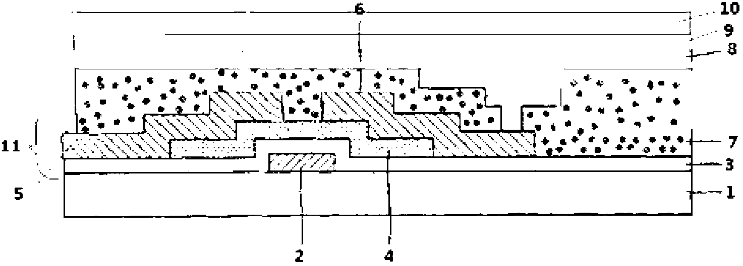
[0080] The structure and preparation method of the TFT device prepared in this embodiment using the above-mentioned metal oxide thin film as a semiconductor layer are as described in Embodiment 1.


PUM

PropertyMeasurementUnit
Wavelengthaaaaaaaaaa
Thicknessaaaaaaaaaa

Abstract

The invention belongs to the field of electron devices and particularly relates to a metallic oxide semiconductor film which is obtained by adopting of laser annealing craft, and application of the metallic oxide semiconductor film in a thin film transistor (TFT) device and an organic light emitting diode (OLED) device. The method of preparing of the metallic oxide semiconductor film includes of (1) preparing the metallic oxide semiconductor film which is based on zinc oxide and formed by adding of other metallic elements; (2), under oxygen atmosphere, the metallic oxide semiconductor film which is obtained in the step (1) conducting laser annealing for 3-6min, and the needed metallic oxide semiconductor film forming. Performance of the metallic oxide semiconductor film, such as migration rate and stability of threshold voltage, is greatly improved, compared with a traditional manner which uses a high-temperature annealing furnace for annealing, efficiency is higher, and stability is better.

Description

technical field [0001] The invention belongs to the field of electronic devices, and in particular relates to a metal oxide thin film obtained by a laser annealing process and its application in TFT and OLED devices. Background technique [0002] Organic light-emitting devices (English full name organic lighting emitting display, referred to as OLED) have the advantages of active light emission, wide color gamut, fast response, wide viewing angle, high contrast ratio, planarization, etc., and are the development trend of the next generation of display and lighting technology. [0003] OLED display devices can be divided into passive matrix OLED (PMOLED) and active matrix OLED (AMOLED) according to the driving method; PMOLED adopts the scanning method, which has the characteristics of instantaneous high brightness, high power consumption, short life, and easy deterioration of display components. , not suitable for large-screen high-resolution lighting and other shortcomings, ...

Claims


Application Information

Patent Timeline
IPC IPC(8): H01L21/336H01L21/268H01L29/786H01L27/32
Inventor 平山秀雄邱勇施露张洁黄秀颀
Owner CHENGDU VISTAR OPTEOLECTRONICS CO LTD
Why Eureka
Try Eureka