Chip engagement device and chip engagement method

A chip bonding and jointing technology, which is applied in the manufacture of electrical components, electrical solid devices, semiconductor/solid devices, etc., can solve the problems of lengthening manufacturing process and hindering cost reduction, so as to ensure the bonding strength and reduce the amount of hydrogen used , the effect of reducing processing costs

Inactive Publication Date: 2013-04-24
HITACHI HIGH TECH INSTR CO LTD
View PDF6 Cites 9 Cited by
  • Summary
  • Abstract
  • Description
  • Claims
  • Application Information

AI Technical Summary

Problems solved by technology

However, since intermittent processing (batsuchi processing) is required for vacuuming, and a cleaning process is required due to flux residue remaining after cooling, the manufacturing process is lengthened, which is a major obstacle to cost reduction.

Method used


Image

  • Chip engagement device and chip engagement method
  • Chip engagement device and chip engagement method
  • Chip engagement device and chip engagement method

Examples


Embodiment 1

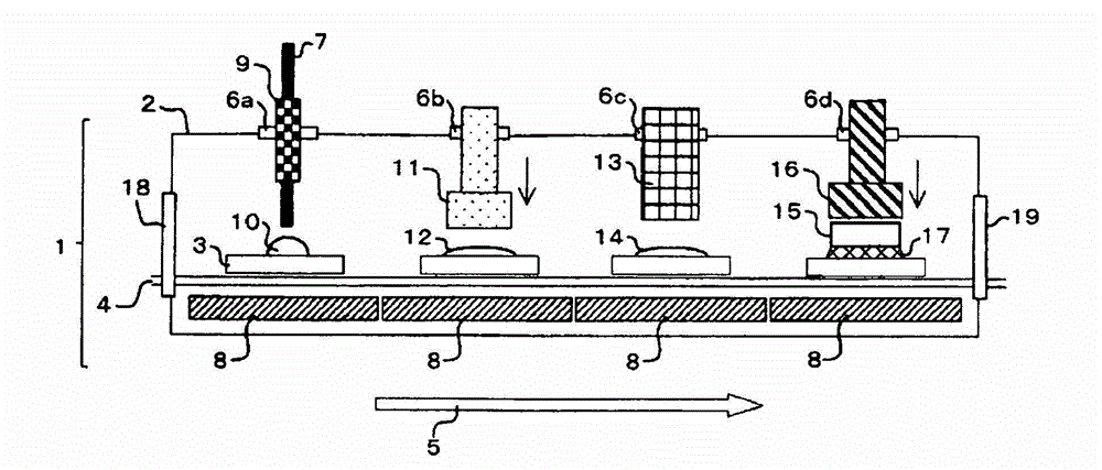
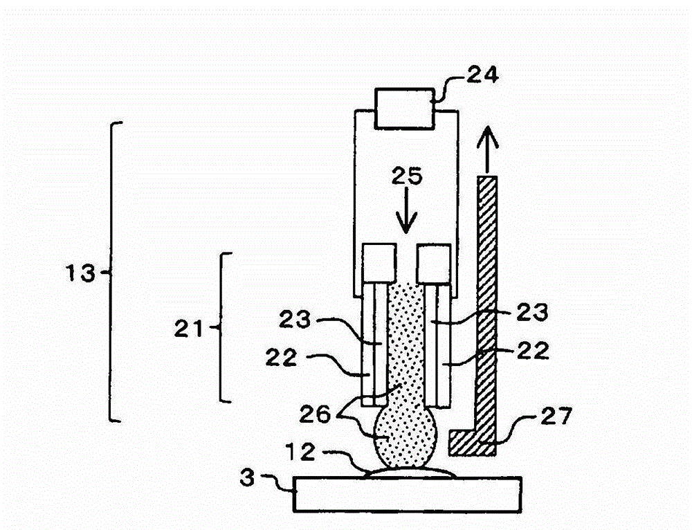
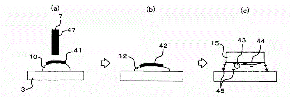
[0045] figure 1 It is an enlarged view of a main part of the die bonder having a solder surface cleaning unit according to the present invention. This die bonding machine 1 is in a furnace covered by a cover 2 to isolate the outside air, and has a guide rail 4 for intermittently moving a lead frame or a substrate 3, which is a member to be bonded, along a moving direction 5 of the lead frame or substrate 3, Four opening windows 6 a , 6 b , 6 c , and 6 d are provided at predetermined positions on the top surface of the cover (furnace) 2 . When described in terms of the die bonding process, the first step is a solder supply step of supplying the elongated solder wire 7 to the lead frame or the substrate 3 through the opening window 6 a. If this step is described in detail, the solder wire 7 sent from the solder supply nozzle 9 contacts the lead frame or the substrate 3 whose bottom surface is heated by the heater 8, and the front end of the solder wire 7 melts and wets the lead...

Embodiment 2

[0074] An example of other solder surface cleaning unit 13 Figure 10 As shown, the surface of the molten solder 12 on the lead frame or substrate 3 is plasma treated using a torch nozzle 31 at atmospheric pressure. In the torch nozzle 31, the center electrode 33 is arranged in the center of the counter electrode 32, and the insulator 34 is provided on the surface of each electrode. A high-frequency power source 35 is connected to the center electrode 33 . In addition, a processing gas is supplied from the gas inlet 36 , plasma is generated in the discharge space 37 , and nozzle-shaped plasma 39 is irradiated from the gas outlet 38 . As the processing gas, a mixed gas of nitrogen and hydrogen used as the ambient gas of the plasma apparatus was used. Thereby, hydrogen plasma is generated, and the oxide film on the surface of the molten solder 12 existing on the lead frame or the substrate 3 can be reduced.

[0075] At this time, reaction products are generated, and if left u...

Embodiment 3

[0078] An example of other solder surface cleaning units Figure 11 shown. This method is a method of irradiating laser beams. Laser beam 102 generated from laser oscillator 101 is irradiated on the surface of molten solder 14 on lead frame or substrate 3 via optical fiber 103, optical lens 104 system, and the like. The furnace is an ambient gas with a low oxygen concentration, and there is also reducing hydrogen, so the oxide film on the surface of the solder can be effectively removed. Here, as laser light, pulsed laser light of YAG laser or excimer laser is used, but not limited thereto. In addition, not only a nozzle shape but also a line shape can be used.

[0079] In addition, when the area of ​​solder to be processed is wide, the laser beam irradiation is not irradiated so that the output is high in the center (convex shape), but is irradiated in a ring shape so that the output is substantially the same as a whole. By irradiating a laser beam, it is also possible to ...


PUM


Abstract

The present invention provides a chip engagement device and a chip engagement method which can reduce voids in a solder engagement portion and poor interface engagement. A chip engagement machine which engages a semiconductor chip on a lead frame or a substrate by the solder comprises a conveying unit for conveying the above lead frame or the substrate, a solder supply unit for supplying the solder to the above lead frame or the substrate, and a carrying unit for carrying and engaging the above semiconductor chip onto the above lead frame or the substrate. The chip engagement machine also has a surface clean unit. The surface clean unit removes an oxide film on the solder surface melt in a furnace after the solder is supplied to the lead frame or the substrate. Chip engagement quality can be increased by the above chip engagement device.

Description

technical field [0001] The present invention relates to a chip bonding device and a chip bonding method. Background technique [0002] In a semiconductor device using a lead frame, generally, a semiconductor chip is mounted on a stage portion of the lead frame, and electrodes of the semiconductor chip and electrodes of the lead frame are electrically connected by methods such as wire bonding. Then, the periphery of the semiconductor chip and the wiring portion such as the wire bonding is molded with resin, and the lead frame portion outside the resin portion is cut into a predetermined lead shape to obtain an individual semiconductor device. [0003] In semiconductor devices, adhesives are often used to connect lead frames and semiconductor chips, but in semiconductor devices that handle large currents, high power, etc., it is necessary to transfer the heat generated by the semiconductor chip to the stage to efficiently use Heat is released to the outside of the semiconduct...

Claims


Application Information

Patent Timeline
Patent Type & Authority Applications(China)
IPC IPC(8): H01L21/60
CPCH01L24/83H01L24/743H01L24/75H01L24/27H01L2224/83192
Inventor 秦英惠福田正行市川良雄牛房信之深谷康太
Owner HITACHI HIGH TECH INSTR CO LTD
Why Eureka
Try Eureka