Wavelength expansion InGaAs detector structure on GaAs substrate

A detector and wavelength technology, used in semiconductor devices, electrical components, circuits, etc., can solve problems such as large dark current, and achieve the effects of reducing manufacturing costs, reducing defect density, and fast relaxation

Inactive Publication Date: 2013-05-01
SHANGHAI INST OF MICROSYSTEM & INFORMATION TECH CHINESE ACAD OF SCI
View PDF3 Cites 7 Cited by
  • Summary
  • Abstract
  • Description
  • Claims
  • Application Information

AI Technical Summary

Problems solved by technology

At present, the detection cut-off wavelength of InP-based InGaAs infrared detectors has been extended to 2.9 μm, and the device has also developed from a unit device to an infrared focal plane array, but the large dark current is still an important problem restricting its application

Method used


Image

  • Wavelength expansion InGaAs detector structure on GaAs substrate
  • Wavelength expansion InGaAs detector structure on GaAs substrate

Examples


Embodiment 1

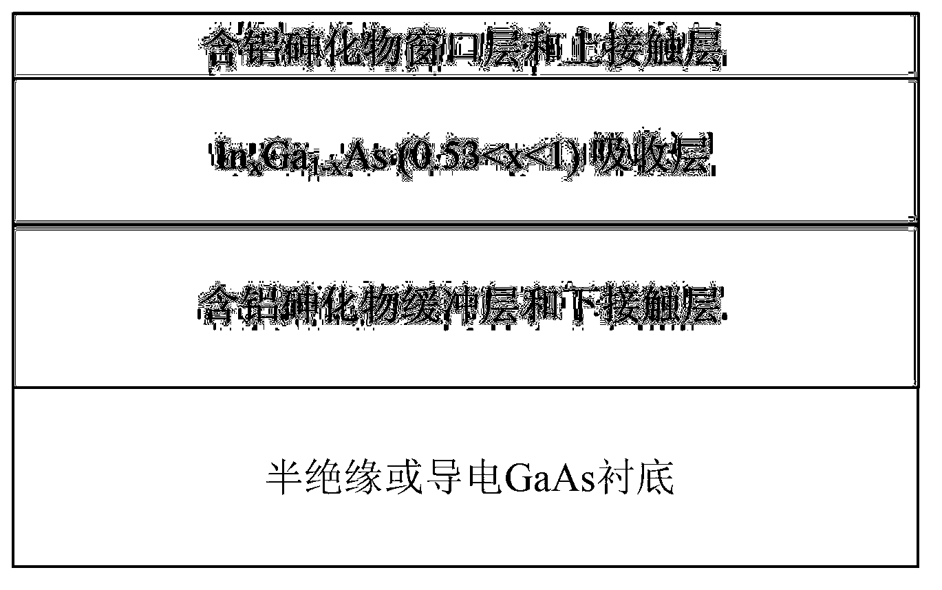
[0018] An InGaAs Detector Structure with a Cutoff Wavelength of 2.4 Microns on a GaAs Substrate

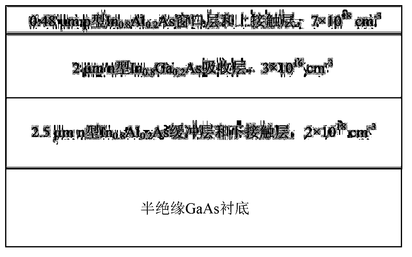
[0019] (1) Use the semi-insulating GaAs single crystal material with [100] crystal orientation as the substrate of the detector, and use the conventional molecular beam epitaxy method to grow highly doped n-type GaAs of about 200nm on the substrate as the buffer layer;

[0020] (2) Then grow highly doped n-type In with a thickness of about 2.5 μm and an In content of 80% 0.8 Al 0.2 As buffer layer with an electron concentration of 2×10 18 cm -3 , the epitaxial layer is used to release the strain and can also serve as the lower contact layer;

[0021] (3) The regrowth thickness is 2 μm, and the electron concentration is 3×10 16 cm -3 Low-doped n-type In 0.8 Ga 0.2 As absorbing layer, and then continue to grow to a thickness of 0.48μm and a hole concentration of 7×10 18 cm -3 Highly doped p-type In 0.8 Ga 0.2 The upper contact layer of As serves as the window layer at the...


PUM


Abstract

The invention relates to a wavelength expansion InGaAs detector structure on a GaAs substrate. The cut-off wavelength of the detector prepared by using the structure is greater than 1.7 micrometers but smaller than 3.5 micrometers, aluminum-containing arsenide materials are arranged on the GaAs substrate in an epitaxy way to be used as a buffer layer and a lower contact layer, InGaAs is used as an absorption layer, and in addition, aluminum-containing arsenide materials are adopted to be used as a window layer and an upper contact layer. The detector structure provided by the invention can expand the application range of the InGaAs detector and the array of the InGaAs detector, the GaAs substrate with maturer process and higher quality is adopted, the device cost can be reduced, the influence on the epitaxial layer hidden current caused by the substrate defects is reduced, the quantum efficiency is improved, and wide application prospects are realized.

Description

technical field [0001] The invention belongs to the field of semiconductor optoelectronic materials and devices, in particular to an extended wavelength InGaAs detector on a GaAs substrate. Background technique [0002] Ternary In x Ga 1-x The As material is a full-component direct bandgap material. By adjusting the In component x, it can cover the 0.8~3.5μm band. Detectors made of InGaAs materials have the advantages of high sensitivity, fast response, good radiation resistance, and room temperature operation, making them ideal materials for space remote sensing in the short-wave infrared band. For detectors used in space remote sensing, the focus of research is to suppress noise, reduce the dark current of the device, and improve the detection rate. At present, the detection cut-off wavelength of InP-based InGaAs infrared detectors has been extended to 2.9 μm, and the device has also developed from a unit device to an infrared focal plane array, but the large dark curre...

Claims


Application Information

Patent Timeline
Patent Type & Authority Applications(China)
IPC IPC(8): H01L31/0304
Inventor 陈星佑顾溢张永刚
Owner SHANGHAI INST OF MICROSYSTEM & INFORMATION TECH CHINESE ACAD OF SCI
Why Eureka
Try Eureka