A kind of preparation method of metal oxide semiconductor nanometer material

A technology of oxide semiconductors and nanomaterials, applied in the field of inorganic nanomaterials, can solve problems such as insufficient product purity and complex processes, and achieve the effects of high product purity, simple experimental equipment requirements, and strong operability

Inactive Publication Date: 2015-10-28
NANJING TECH UNIV
View PDF2 Cites 0 Cited by
  • Summary
  • Abstract
  • Description
  • Claims
  • Application Information

AI Technical Summary

Problems solved by technology

However, most of these synthetic methods still have obvious deficiencies, such as insufficient product purity, complicated process, etc.

Method used


Image

  • A kind of preparation method of metal oxide semiconductor nanometer material
  • A kind of preparation method of metal oxide semiconductor nanometer material
  • A kind of preparation method of metal oxide semiconductor nanometer material

Examples


Embodiment 1

[0029] Example 1 Preparation of beam-shaped copper oxide nanomaterials

[0030] 1) Preparation of copper electrode pairs

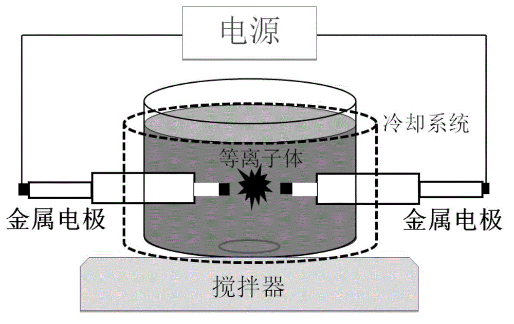
[0031] Select two copper rods with a diameter of 2mm and a length of 10mm, put an alumina insulating tube (inner diameter 2mm, outer diameter 3mm) on the two copper rods, and then fix them in a Teflon tube (inner diameter 3mm) to obtain a copper reaction electrode . Install the above-mentioned copper reaction electrode on the glass container through the hole on the container wall in a horizontally opposite position. The distance between the electrode pairs is fixed at 0.2mm, and the angle between the electrode pairs is fixed at 180°. Connect a pulsed DC power supply (model MPP- HV03, Japan Co., Ltd. Kurita Manufacturing Co., Ltd.) to form a discharge circuit.

[0032] 2) Preparation of beam-like copper oxide nanomaterials

[0033] Add 120ml of distilled water into a 150ml glass container to ensure that the copper electrode pair is submerged in water and...

Embodiment 2

[0037] Example 2 Preparation of flower cluster zinc oxide nanomaterials

[0038] 1) Preparation of zinc electrode pair:

[0039] Select two zinc wires with a diameter of 1mm and a length of 10mm, put an aluminum oxide insulating tube (inner diameter 1mm, outer diameter 2.5mm) on the two zinc wires, and then fix them in a Teflon tube (inner diameter 2.5mm) to obtain zinc Reactive electrodes. Install the above-mentioned zinc reaction electrode on the glass container through the hole on the container wall in a horizontally opposite position, the distance between the electrode pairs is fixed at 0.2mm, the angle between the electrode pairs is fixed at 180°, and a pulsed DC power supply (model MPP- HV03, Japan Co., Ltd. Kurita Manufacturing Co., Ltd.) to form a discharge circuit. Then if figure 1 Place the glass container in a room temperature water bath as indicated.

[0040] 2) Preparation of flower cluster ZnO nanomaterials

[0041]Add 120ml of distilled water into a 150ml g...


PUM


Abstract

The invention relates to a preparation method of a novel metal oxide semiconductor nano-material. The preparation method comprises the following steps: supplying power for two metal electrodes placed in water through a pulse direct-current source for generating plasma discharge between the two electrodes, carrying out continuous sputtering attack of the surfaces of the metal electrodes through high-energy plasma generated through discharge, allowing metal atoms or metal atom clusters formed on the surfaces of the electrodes to enter water, and carrying out in-situ oxidation and adhesion to form the metal oxide nano-material having a unique morphology. The method which is operated in a normal-temperature normal-pressure open system has the advantages of simple experiment equipment requirements, strong maneuverability and high product purity.

Description

technical field [0001] The invention belongs to the field of inorganic nanometer materials, in particular to a preparation method of copper oxide and zinc oxide semiconductor nanomaterials. Background technique [0002] The physical and chemical properties of nanoscale metal oxide semiconductors are very different from those of bulk materials, so the research on metal oxide semiconductor nanomaterials has received great attention. [0003] Copper oxide (CuO) and zinc oxide (ZnO) are two important semiconducting materials, which have applications in the fields of catalysts, gas-phase and biosensors, nanostructured varistors, UV absorbers, dye-sensitized solar cells, light-emitting diodes, hydrogen storage, etc. Wide range of applications. In the research and application, it is found that after entering the nanoscale, the particle size and morphology have a great influence on the physical and chemical properties of semiconductor compounds and their application directions. The...

Claims


Application Information

Patent Timeline
Patent Type & Authority Patents(China)
IPC IPC(8): C25D11/02B82Y40/00
Inventor 胡秀兰
Owner NANJING TECH UNIV
Why Eureka
Try Eureka