Nanowire semiconductor gas sensitive material based on GaN-Ga2O3 core-shell structure

A gas-sensitive material and core-shell structure technology, applied in the direction of material resistance, etc., can solve the problems of sensor performance stability and signal repeatability, sensor cost increase, high process requirements, etc., to achieve easy size, reduce preparation costs, The effect of high sensitivity

Inactive Publication Date: 2013-05-15
DALIAN UNIV OF TECH
View PDF4 Cites 7 Cited by
  • Summary
  • Abstract
  • Description
  • Claims
  • Application Information

AI Technical Summary

Problems solved by technology

However, because the nanoparticles are small and have a large active specific surface area, they are prone to agglomeration after long-term use under high temperature or other similar environments, resulting in poor sensor performance stability and signal repeatability
While a single Ga with a one-dimensional structure 2 o 3 Although nanowires can overcome the above-mentioned problem of particle agglomeration and maintain the high sensitivity of the sensor, under the existing process conditions, Ga 2 o 3 Nanowires have high requirements on the process, resulting in a significant increase in the cost of the sensor

Method used


Image

  • Nanowire semiconductor gas sensitive material based on GaN-Ga2O3 core-shell structure
  • Nanowire semiconductor gas sensitive material based on GaN-Ga2O3 core-shell structure

Examples


Embodiment Construction

[0010] The specific embodiments of the present invention will be described in detail below in conjunction with the technical solutions and accompanying drawings.

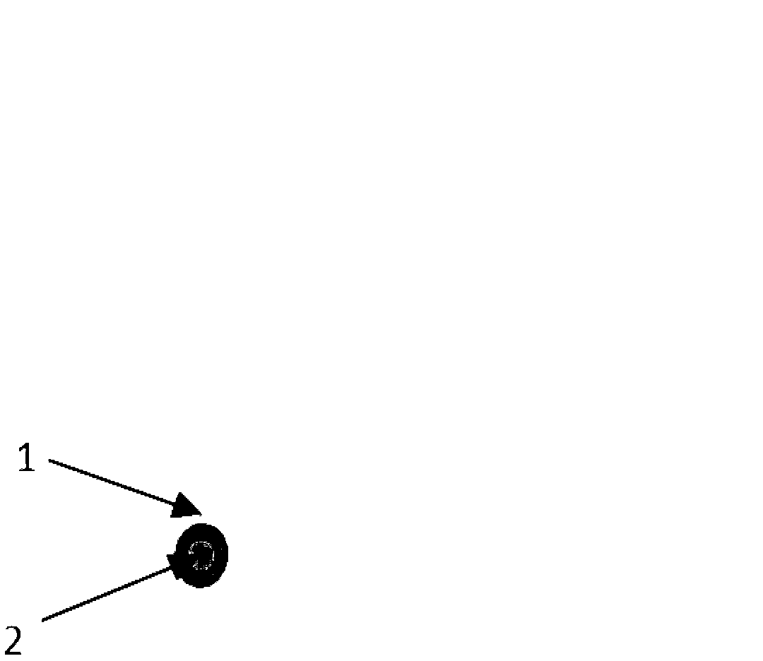
[0011] MOCVD preparation of core-shell nanowire-sensitive materials: Si wafers are used as substrates, and a layer of 1-5nm metal Ni is first sputtered on the substrate, and then the wafers are placed in the quartz boat of the reactor, and NH 3 As nitrogen source, trimethylgallium as gallium source, at 900 o C high temperature through H 2 Under the condition of growing 5-30min, obtain the diameter 50-500nm, the GaN nanowire that length is 3-50 micron; Then gain nanowire in 200 o C to 1000 o C high temperature through O 2 Oxidation under atmosphere, reasonable control of O 2 Concentration and oxidation time, a layer of Ga with a thickness of 5-20nm is grown on the periphery of GaN nanowires 2 o 3 layer, to obtain GaN-Ga with a core-shell structure 2 o 3 nanowire gas-sensing materials.

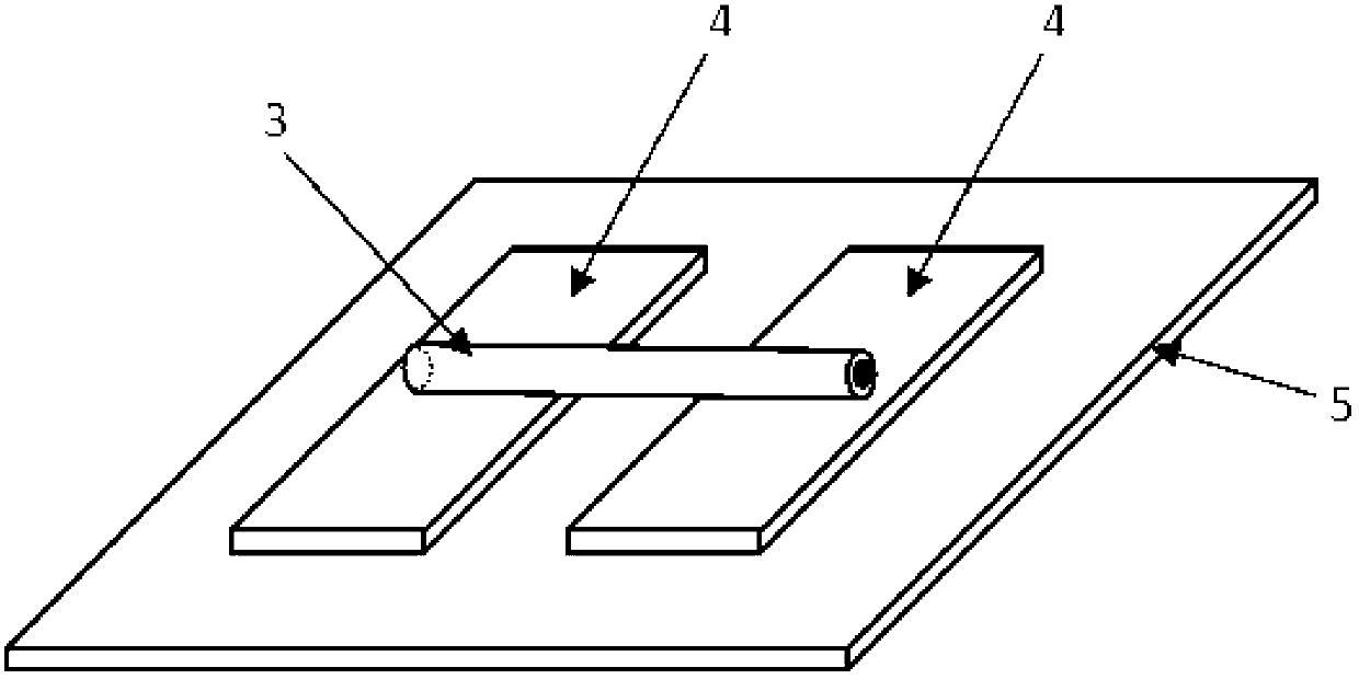
[0012] Gas-sensing pe...


PUM

PropertyMeasurementUnit
diameteraaaaaaaaaa
thicknessaaaaaaaaaa
diameteraaaaaaaaaa

Abstract

The invention relates to a nanowire semiconductor gas sensitive material based on a GaN-Ga2O3 core-shell structure, belonging to the technical field of electron gas sensitive devices. The nanowire semiconductor gas sensitive material is characterized in that the surface layer of a GaN nanowire with diameter of 50-500nm is oxidized at high temperature into a layer of Ga2O3 with the thickness of 5-20nm, so that a nanowire semiconductor gas sensitive material with the GaN-Ga2O3 core-shell structure is obtained, and the nanowire semiconductor gas sensitive material with the GaN-Ga2O3 core-shell structure can be used for detecting gases with harmful neuron, such as oxygen, heavy hydrogen, hydrogen sulfurous gas, nitric oxide, various hydrocarbon gases and ammonia. The nanowire semiconductor gas sensitive material has the beneficial effects that the size of a carrier nanowire is easy to manufacture, the thickness of the Ga2O3 sensitive material obtained through oxidation is 5-20nm, which approximates to the size of a debye depletion layer, so that response of high sensitivity to the gas is obtained, the problem of direction preparation of Ga2O3 nanowire with diameter of 5-20nm is solved, the preparation cost is further lowered, and the cost is saved.

Description

technical field [0001] The invention belongs to the technical field of electronic gas sensor and relates to a GaN-Ga based 2 o 3 Core-shell structure nanowire semiconductor gas-sensing material. Background technique [0002] Ga 2 o 3 It is a good semiconductor metal oxide gas-sensing material for O 2 , H 2 And a variety of hydrocarbon gases have a good response. Generally, the smaller the particle size of this type of gas-sensitive material, the higher the response sensitivity to gas detection. Ga 2 o 3 The main nanostructures include nanoparticles and nanowires. Ga 2 o 3 The particle size of the nanoparticles can reach 10-20nm, which is close to the Debye surface depletion size, so that a large sensing signal can be obtained. However, because the nanoparticles are small and have a large active specific surface area, they are prone to agglomeration after long-term use under high temperature or other similar environments, resulting in poor sensor performance stabi...

Claims


Application Information

Patent Timeline
Patent Type & Authority Applications(China)
IPC IPC(8): G01N27/04
Inventor 李晓干刘丽鹏黄辉王兢朱慧超唐祯安闫卫平
Owner DALIAN UNIV OF TECH
Why Eureka
Try Eureka