

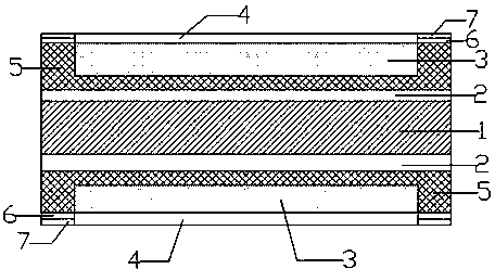
Manufacturing technique of low-voltage chip and low-voltage chip thereof
A production process and chip technology, applied in the field of chip production and preparation, can solve the problems of large leakage of low-voltage chips, product failure, and inability to passivate, etc., and achieve the effect of increasing the diffusion gradient, reducing the leakage value, and steeping the diffusion gradient
- Summary
- Abstract
- Description
- Claims
- Application Information
AI Technical Summary
Problems solved by technology
Method used
Image

Examples
Embodiment 1
[0032] A production process for a low-voltage chip, comprising the following steps:
[0033] (1) Select P-type original silicon wafer: select a P-type original silicon wafer with a resistivity of 0.002 ohm / cm and a thickness of 290 microns;
[0034] (2) Pretreatment before the diffusion of boron impurities: firstly, the P-type raw silicon wafer selected in step (1) is placed in a mixed acid composed of nitric acid, hydrofluoric acid and glacial acetic acid at a temperature of 1-3°C. Carry out chemical etching for 30 seconds, wherein the volume ratio of nitric acid: hydrofluoric acid: glacial acetic acid is 18:1:1; then the P-type original silicon wafer is rinsed in pure water and placed in a hydrogen peroxide, ammonia and water ratio. Heat up the prepared No. 1 solution to wash the P-type raw silicon wafer at 80°C for 10 minutes, wherein the volume ratio of hydrogen peroxide: ammonia water: water is 1:1:6; rinse with water after cleaning in No. 1 solution Clean, and then plac...
Embodiment 2
[0047] A production process for a low-voltage chip, comprising the following steps:
[0048] (1) Select P-type original silicon wafer: select a P-type original silicon wafer with a resistivity of 0.0037 ohm / cm and a thickness of 340 microns;
[0049] (2) Pretreatment before the diffusion of boron impurities: firstly, the P-type raw silicon wafer selected in step (1) is placed in a mixed acid composed of nitric acid, hydrofluoric acid and glacial acetic acid at a temperature of 1-3°C. Carry out chemical etching for 30 seconds, wherein the volume ratio of nitric acid: hydrofluoric acid: glacial acetic acid is 18:1:1; then the P-type original silicon wafer is rinsed in pure water and placed in a hydrogen peroxide, ammonia and water ratio. Heating in the prepared No. 1 solution, and cleaning the P-type raw silicon wafer at 95°C for 10 minutes, wherein the volume ratio of hydrogen peroxide: ammonia water: water is 1:1:6; rinse with water after cleaning in No. 1 solution Clean, and...
Embodiment 3
[0062] A production process for a low-voltage chip, comprising the following steps:
[0063] (1) Select P-type original silicon wafer: select a P-type original silicon wafer with a resistivity of 0.0035 ohm / cm and a thickness of 310 microns;
[0064] (2) Pretreatment before the diffusion of boron impurities: firstly, the P-type raw silicon wafer selected in step (1) is placed in a mixed acid composed of nitric acid, hydrofluoric acid and glacial acetic acid at a temperature of 1-3°C. Carry out chemical etching for 30 seconds, wherein the volume ratio of nitric acid: hydrofluoric acid: glacial acetic acid is 18:1:1; then the P-type original silicon wafer is rinsed in pure water and placed in a hydrogen peroxide, ammonia and water ratio. Heating in the prepared No. 1 liquid to heat up the P-type raw silicon wafer at 90°C for 10 minutes, wherein the volume ratio of hydrogen peroxide: ammonia water: water is 1:1:6; rinse with water after cleaning in No. 1 liquid Clean, and then p...
PUM
 Abstract
Description
Claims
Application Information