Light-emitting diode (LED) epitaxial wafer

An LED epitaxial wafer, N-type technology, applied in the direction of electrical components, circuits, semiconductor devices, etc., can solve the problems of uneven current distribution, low effect and brightness, and current congestion in the epitaxial layer, and achieve the enhancement and improvement of electronic horizontal expansion capabilities Brightness and light efficiency, the effect of reducing the driving voltage

Active Publication Date: 2013-05-15
XIANGNENG HUALEI OPTOELECTRONICS
View PDF3 Cites 17 Cited by
  • Summary
  • Abstract
  • Description
  • Claims
  • Application Information

AI Technical Summary

Problems solved by technology

[0005]However, there are outstanding shortcomings in this structure
For example, due to the use of continuously doped GaN layers with Si, the amount of dopant Si is too high
Moreover, the traditional N-type GaN layer, because the doping Si concentration is the same, the resistance value of each place is the same
This makes the electron transportation process choose the shortest path for transmiss

Method used


Image

  • Light-emitting diode (LED) epitaxial wafer
  • Light-emitting diode (LED) epitaxial wafer
  • Light-emitting diode (LED) epitaxial wafer

Examples


Embodiment approach 1

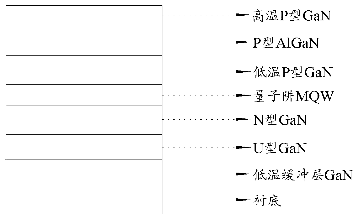
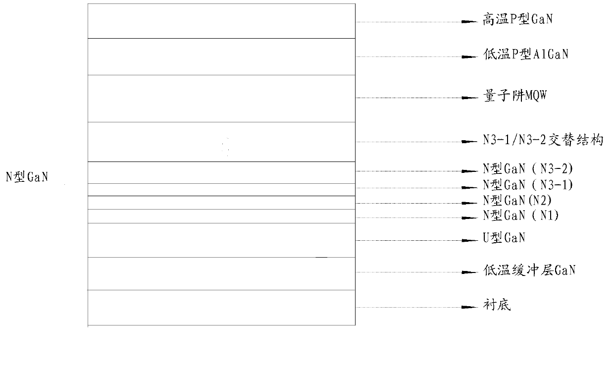
[0034] Prepare sample 1 according to the traditional way, its structure is as figure 1 shown. In addition, sample 2 was prepared according to the present invention, and its structure is as figure 2 shown. The difference between sample 1 and sample 2 is that sample 2 uses 16 alternate structural layers composed of N3-1 layer and N3-2 layer instead of the N3 layer in sample 1, and details can be referred to Table 1. Sample 1 and sample 2 were plated with an ITO layer of 200nm under the same pre-process conditions, a Cr / Pt / Au electrode of 130nm under the same conditions, and a protective layer of SiO2 under the same conditions. 2 About 50nm, and then under the same conditions, the sample was ground and cut into chip particles of 762μm×762μm (30mi×30mil), and then sample 1 and sample 2 each selected 150 crystal grains at the same position. Under the same packaging process, Packaged into a white LED. Then an integrating sphere was used to test the photoelectric properties of s...

Embodiment approach 2

[0039] Sample 3 was prepared according to the traditional way, and its structure is as figure 1 shown. In addition, sample 4 was prepared according to the present invention, its structure is as figure 2 shown. The difference between sample 3 and sample 4 is that sample 4 uses 15 alternate structural layers consisting of N3-1 layer and N3-2 layer instead of the N3 layer in sample 3, see Table 2 for details. Samples 3 and 4 were plated with 180nm of ITO layer under the same pre-process conditions, 120nm of Cr / Pt / Au electrodes were plated under the same conditions, and the protective layer of SiO was plated under the same conditions. 2 About 50nm, then grind and cut the sample into chip particles of 250μm×457μm (10mi×18mil) under the same conditions, then select 150 crystal grains at the same position for sample 3 and sample 4, and package them under the same packaging process into a white LED. Then an integrating sphere was used to test the photoelectric properties of sampl...


PUM

PropertyMeasurementUnit
Thicknessaaaaaaaaaa
Thicknessaaaaaaaaaa
Thicknessaaaaaaaaaa

Abstract

Disclosed is a light-emitting diode (LED) epitaxial wafer. The LED epitaxial wafer sequentially comprises a substrate, a gallium nitride (GaN) buffering layer, a non-dopant GaN layer, a doped N type GaN layer with silicon (Si), an indium gallium nitride (InGaN)/GaN multiple quantum well layer, a P type aluminum gallium nitride (AlGaN) layer and a P type doped GaN layer with magnesium (Mg), wherein the doped GaN layer with Si comprises a first doped N type GaN layer with Si, a second doped N type GaN layer with Si and at least one alternate structure layer composed of a third doped N type GaN layer with Si and an undoped U type GaN layer with no Si. According to the alternate structure layer composed of the third doped N type GaN layer with Si and the undoped U type GaN layer with no Si, usage amount of dopant is reduced, a driving voltage is reduced, and luminance and a lighting effect are improved.

Description

technical field [0001] The invention relates to an LED epitaxial wafer. Background technique [0002] At present, large-size and high-power chips with specifications of 30mil×30mil and 45mil×45mil are used in street lighting, and small and medium-sized chips with specifications of 10mil×18mil and 10mil×23mil are used in backlight sources. The heat dissipation of large-size chips is an important indicator. The luminous performance of large-size chips is no longer defined by high lumens. The market value of high-power is oriented to lumens / (watts x unit price), and small and medium-sized chips do not need to consider heat dissipation. The market The value orientation is lumens / unit price. [0003] Currently, there are various structures of epitaxial wafers, which achieve the purpose of improving light efficiency and brightness by designing quantum wells and P-type layers. For example, in some structures, the superlattice structures such as PAlGaN / PInGaN, PAlGaN / PGaN, PAlGaN / ...

Claims


Application Information

Patent Timeline
IPC IPC(8): H01L33/14
Inventor 张宇
Owner XIANGNENG HUALEI OPTOELECTRONICS
Why Eureka
Try Eureka