High-resolution electron energy loss spectrometer for energy and momentum two-dimensional analyses
A technology of electron energy loss and electron energy analysis, applied in instruments, measuring devices, scientific instruments, etc., to achieve the effects of high detection efficiency, improved detection efficiency, and high-precision data acquisition performance
- Summary
- Abstract
- Description
- Claims
- Application Information
AI Technical Summary
Problems solved by technology
Method used
Image
Examples
Embodiment 1
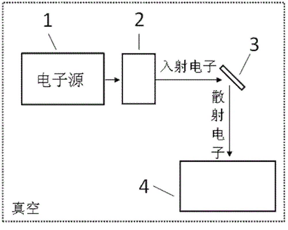
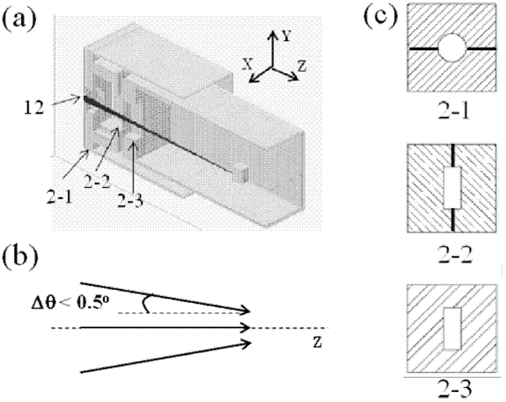
[0056] refer to Figure 4 , this type of spectrometer includes the following devices: (1) low-energy electron excitation source system, mainly composed of hot cathode LaB 6 Filament 6, filament lens group 7, slit 8, pre-stage fan-shaped monochromator 9, slit 10, fan-shaped monochromator 11, exit slit 12, high-precision electron source rotating platform 5, etc. (2) Angle resolution mode exit lens unit 2 is mainly composed of a first electrode 2-1, a second electrode 2-2, a third electrode 2-3 and the like. (3) Angle-resolved electronic energy analyzer, mainly including electronic receiver, angle-resolved lens group 13, analyzer incident slit 14, hemispherical energy analyzer 15 and so on. (4) Signal receiving and data acquisition system, including microchannel plate electron multiplier (MCP) 16 or DLD, charge-coupled device (CCD) 17 and data acquisition system 18 .
[0057] The electron beam that exits from fan-shaped monochromator 11, exit slit 12 has approximately rectangul...
Embodiment 2
[0071] refer to Figure 5 , this type of spectrometer includes the following devices: (1) low-energy electron excitation source system, mainly composed of GaAs photocathode 19, pulsed laser 23, 90° fan-shaped monochromator 20, 180° fan-shaped monochromator 21, exit lens system 2, etc. Composition; (2) tube lens type angle-resolved electron energy analyzer 22; (3) signal receiving and data acquisition system, including microchannel plate electron multiplier (MCP) 16 or DLD, charge-coupled device (CCD) 17 and data acquisition System 18.
[0072] Its working process: (1) pulsed laser 23 sends a pulsed laser light and strikes on the GaAs photocathode 19, and GaAs 19 emits photoelectrons with the same starting time, and the photoelectrons enter the 90° fan-shaped monochromator 20 and the 180° fan-shaped monochromator 21 , under the joint action of the monochromator and the corresponding slit, the energy monochromatization and beam spot shape of the electron beam will be optimized,...
PUM
| Property | Measurement | Unit |
|---|---|---|
| thickness | aaaaa | aaaaa |
| thickness | aaaaa | aaaaa |
| thickness | aaaaa | aaaaa |
Abstract
Description
Claims
Application Information


