

Gallium-nitride-based high electronic mobility transistor structure with barrier layer and manufacture method thereof
A high electron mobility, gallium nitride-based technology, applied in the field of GaN-based high electron mobility transistor structure and fabrication with a barrier layer, can solve the problems of increased interface roughness, reduced mobility, enhanced scattering, etc. , to achieve high two-dimensional electron gas surface density, increase the barrier height, and reduce the effect of process steps
- Summary
- Abstract
- Description
- Claims
- Application Information
AI Technical Summary
Problems solved by technology
Method used
Image

Examples
Embodiment
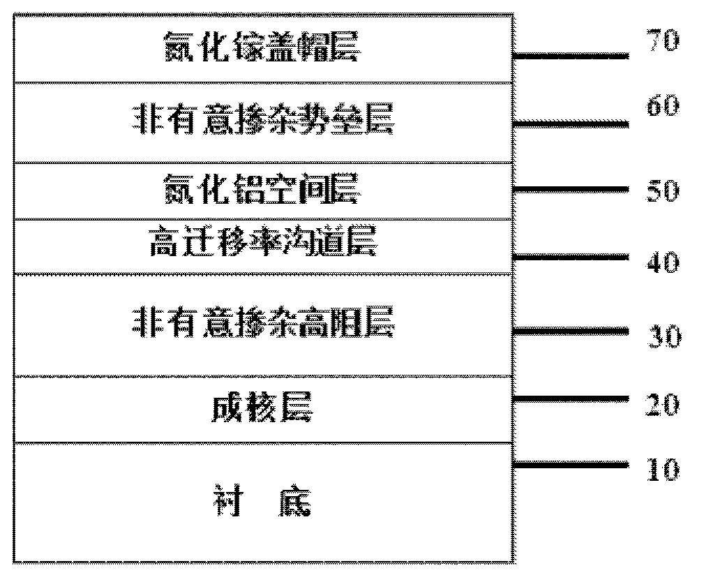
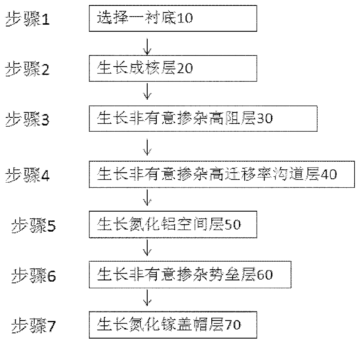
[0045] The present invention provides a GaN-based HEMT structure with a barrier layer, which includes:
[0046] A substrate 10, the material of which is sapphire.
[0047] A nucleation layer 20 is formed on the substrate 10 . The material of the nucleation layer 20 is low-temperature gallium nitride with a thickness of 100 nm;
[0048] An unintentionally doped high-resistance layer 30 is fabricated on the nucleation layer 20 . The aluminum composition y of the unintentionally doped high resistance layer 30 is 0, the material of the unintentionally doped high resistance layer 30 is gallium nitride, and the thickness is 3 μm.
[0049] An unintentionally doped high mobility channel layer 40 is fabricated on the unintentionally doped high resistance layer 30 . The material of the non-intentionally doped high-mobility layer channel layer 40 is gallium nitride with a thickness of 30 nm.
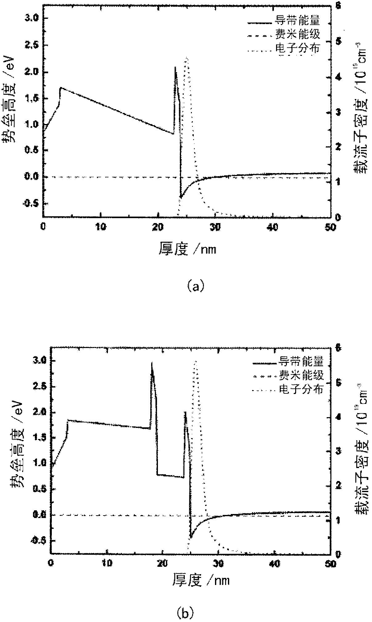
[0050] An unintentionally doped AlN space layer 50 , the unintentionally doped AlN space la...
PUM
| Property | Measurement | Unit |
|---|---|---|
| Thickness | aaaaa | aaaaa |
| Thickness | aaaaa | aaaaa |
| Total thickness | aaaaa | aaaaa |
Abstract
Description
Claims
Application Information