Aluminum-induced crystallization polycrystalline silicon thin-film solar cell and preparation method thereof

A technology of polycrystalline silicon thin film and solar cells, which is applied in circuits, photovoltaic power generation, electrical components, etc., can solve the problems of inability to crystallize silicon thin films, low efficiency, low production efficiency and low battery efficiency, and saves the cost of raw materials and has good application prospects. , the effect of reducing thickness

Active Publication Date: 2013-06-05
JIANGSU LONGBAO ELECTRONICS SCI & TECH CO LTD
View PDF7 Cites 10 Cited by
  • Summary
  • Abstract
  • Description
  • Claims
  • Application Information

AI Technical Summary

Problems solved by technology

The solid-phase crystallization process takes 10-100 hours, and the efficiency is low; laser crystallization is affected by the laser penetration depth, and cannot crystallize thicker silicon films
However, polysilicon is an indirect bandgap semiconductor. How to improve the photon absorption efficiency of the absorbing layer without increasing the thickness of the silicon film is a difficult problem at present.
Although polycrystalline silicon thin film batteries can be prepared on glass substrates, the production efficiency and battery efficiency are lower than those of crystalline silicon batteries and amorphous silicon thin film batteries

Method used


Image

  • Aluminum-induced crystallization polycrystalline silicon thin-film solar cell and preparation method thereof
  • Aluminum-induced crystallization polycrystalline silicon thin-film solar cell and preparation method thereof
  • Aluminum-induced crystallization polycrystalline silicon thin-film solar cell and preparation method thereof

Examples


Embodiment 1

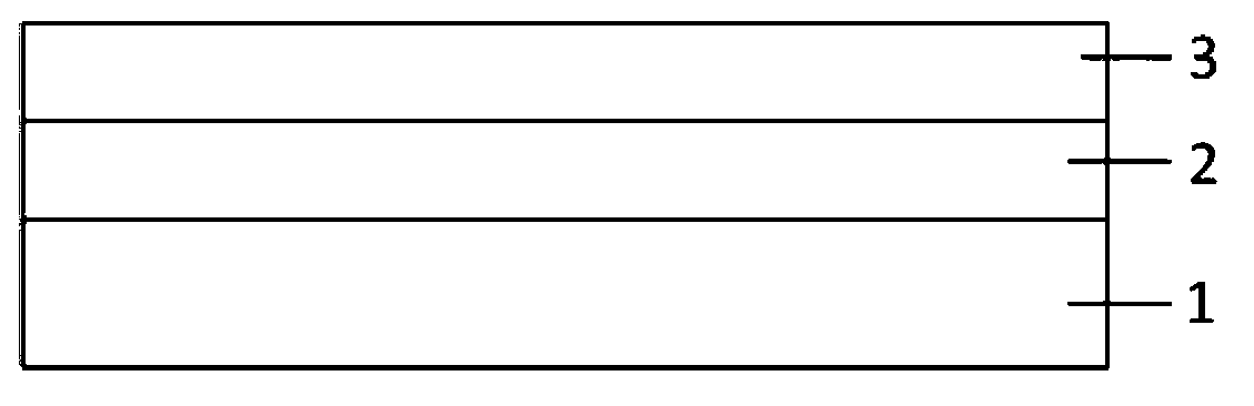
[0026] (1) if figure 1 As shown, a piece of ultra-clear float glass with a size of 150×150×3 mm is selected as the substrate 1 of a polysilicon thin film battery, and an amorphous silicon thin film 2 is grown by PECVD. PECVD process conditions: background vacuum higher than 10 -7 Torr, substrate temperature 150-180°C, pressure 0.36-0.5Torr, RF power 2.5-20W, frequency 13.56MHz, gas SiH 4 The flow rate is 4-10 sccm, and the thickness of the amorphous silicon thin film 2 is 100-150 nm.

[0027] (2) Aluminum thin film 3 is subsequently deposited by magnetron sputtering. Sputtering process conditions: the background vacuum is higher than 10 -7 Torr, the substrate temperature is room temperature, the pressure is 0.005-0.01Torr, the radio frequency power is 100-200W, the frequency is 13.56MHz, the gas Ar flow rate is 10-20sccm, and the thickness of the aluminum film 3 is 100-120nm.

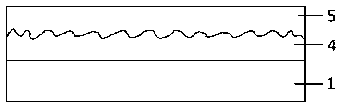
[0028] (3) Anneal the double-layer film in a vacuum annealing furnace, and after annealing at 45...

Embodiment 2

[0031] (1) if figure 1 As shown, a piece of ultra-clear float glass with a size of 150×150×3 mm is selected as the substrate 1 of a polysilicon thin film battery, and an amorphous silicon thin film 2 is grown by PECVD. PECVD process conditions: background vacuum higher than 10 -7 Torr, substrate temperature 150-180°C, pressure 0.36-0.5Torr, RF power 2.5-20W, frequency 13.56MHz, gas SiH 4 The flow rate is 4-10 sccm, and the thickness of the amorphous silicon thin film 2 is 100-150 nm.

[0032] (2) Aluminum thin film 3 is subsequently deposited by magnetron sputtering. Sputtering process conditions: the background vacuum is higher than 10 -7 Torr, the substrate temperature is room temperature, the pressure is 0.005-0.01Torr, the radio frequency power is 100-200W, the frequency is 13.56MHz, the gas Ar flow rate is 10-20sccm, and the thickness of the aluminum film 3 is 100-120nm.

[0033] (3) Anneal the obtained double-layer film in a vacuum annealing furnace. After annealing ...


PUM

PropertyMeasurementUnit
particle sizeaaaaaaaaaa
thicknessaaaaaaaaaa
thicknessaaaaaaaaaa

Abstract

The invention discloses an aluminum-induced crystallization polycrystalline silicon thin-film solar cell and a preparation method of the aluminum-induced crystallization polycrystalline silicon thin-film solar cell and belongs to the field of silicon thin-film solar cells. A structure of the aluminum-induced crystallization polycrystalline silicon thin-film solar cell comprises a glass substrate, a metallic aluminum back reflecting layer, a P+ type back surface field layer, a P type absorption layer and a N+ type transmission layer. Metal electrodes are arranged on the P+ type back surface field layer and the N+ type transmission layer. The preparation method includes the following steps of sequentially depositing an amorphous silicon thin film and an aluminum film through an aluminum-induced crystallization technology, wherein the thickness range is between 100 nm-150nm and 100nm-120nm, conducting annealing process for 1-5 hours at a temperature of 450DEG C-500DEG C, wherein positions of a silicon layer and an aluminum layer can exchange and amorphous silicon is changed into polycrystalline silicon with a grain size of 5mu-10mu, and preparing the P type absorption layer, the N+ type transmission layer and the metal electrodes. The aluminum-induced crystallization polycrystalline silicon thin-film solar cell and the preparation method of the aluminum-induced crystallization polycrystalline silicon thin-film solar cell can theoretically reduce the thickness of an original cell by 50% and greatly save cost of raw materials.

Description

technical field [0001] The invention relates to an aluminum-induced crystallization polycrystalline silicon thin-film cell structure and a preparation method, belonging to the field of crystalline silicon thin-film solar cells. Background technique [0002] Today's traditional fossil energy is increasingly depleted, and solar power generation, as an environmentally friendly and clean energy technology, is bound to become a key development direction in the future. Silicon materials have the characteristics of suitable bandgap width, high photoelectric conversion efficiency, environmentally friendly and low-cost raw materials, and easy industrialization. Therefore, silicon-based solar cells are currently the most widely used type of solar cell technology. Silicon-based solar cells mainly include crystalline silicon solar cells and amorphous silicon thin-film solar cells, each of which has its own advantages and disadvantages. Crystalline silicon batteries have high photoelect...

Claims


Application Information

Patent Timeline
Patent Type & Authority Applications(China)
IPC IPC(8): H01L31/068H01L31/075H01L31/0352H01L31/18H01L31/20
CPCY02E10/50Y02E10/546Y02E10/548Y02P70/50
Inventor 张铭王涛严辉沈华龙王波宋雪梅朱满康侯育冬刘晶冰汪浩
Owner JIANGSU LONGBAO ELECTRONICS SCI & TECH CO LTD
Why Eureka
Try Eureka