Supercharge Your Innovation With Domain-Expert AI Agents!

Manufacture method of metal grid of transistor of complementary metal-oxide-semiconductor (CMOS)

A technology of metal gates and manufacturing methods, which is applied in semiconductor/solid-state device manufacturing, semiconductor devices, electrical components, etc., can solve the problems of multiple grinding residues, prolonging the process time, and reducing the thickness of the metal dielectric layer, so as to reduce grinding residues material, simplify the process flow, and reduce the effect of grinding damage

Active Publication Date: 2013-06-19
SEMICON MFG INT (SHANGHAI) CORP
View PDF2 Cites 2 Cited by
  • Summary
  • Abstract
  • Description
  • Claims
  • Application Information

AI Technical Summary

Problems solved by technology

A common method is to first remove the first dummy gate and form the first work function metal layer and the first filling metal gate in the trench formed by it, and then perform the first chemical mechanical polishing; then, remove the other dummy gate pole and form the second work function metal layer and the second filling metal gate in the trench formed by it, and then perform chemical mechanical polishing for the second time, two or more chemical mechanical polishing processes not only increase the process steps, The process time is prolonged, and multiple chemical mechanical polishing will cause more grinding residues, and greatly damage the interlayer dielectric layer, making the thickness of the metal dielectric layer thinner, thereby affecting the performance of CMOS transistors

Method used


Image

  • Manufacture method of metal grid of transistor of complementary metal-oxide-semiconductor (CMOS)
  • Manufacture method of metal grid of transistor of complementary metal-oxide-semiconductor (CMOS)
  • Manufacture method of metal grid of transistor of complementary metal-oxide-semiconductor (CMOS)

Examples


Embodiment Construction

[0028] In order to make the content of the present invention clearer and easier to understand, the content of the present invention will be further described below in conjunction with the accompanying drawings. Of course, the present invention is not limited to this specific embodiment, and general replacements known to those skilled in the art are also covered within the protection scope of the present invention.

[0029] Secondly, the present invention is described in detail by means of schematic diagrams. When describing the examples of the present invention in detail, for the convenience of explanation, the schematic diagrams are not partially enlarged according to the general scale, which should not be used as a limitation of the present invention.

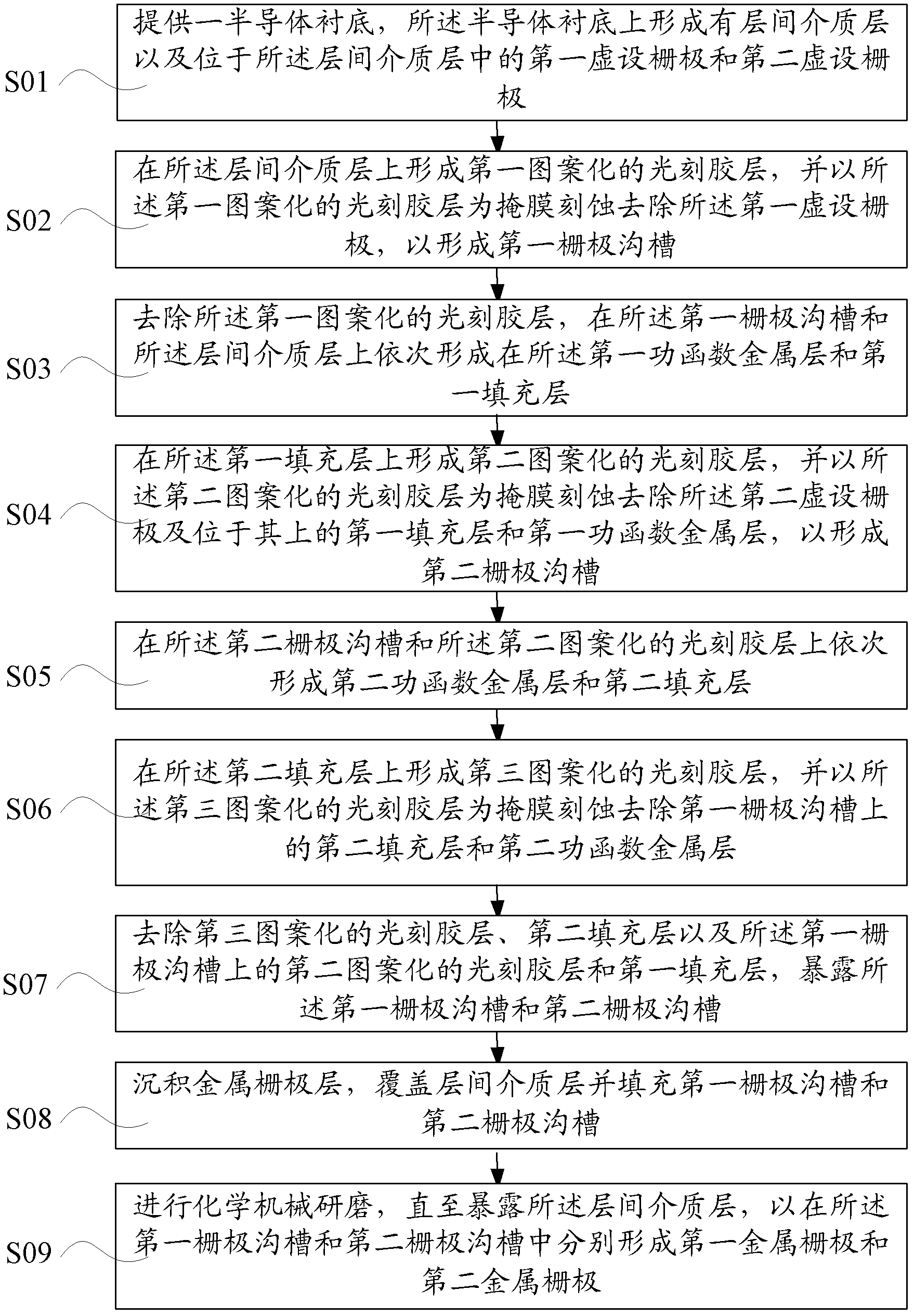
[0030] The invention provides a method for manufacturing a metal gate of a CMOS transistor, comprising the following steps:

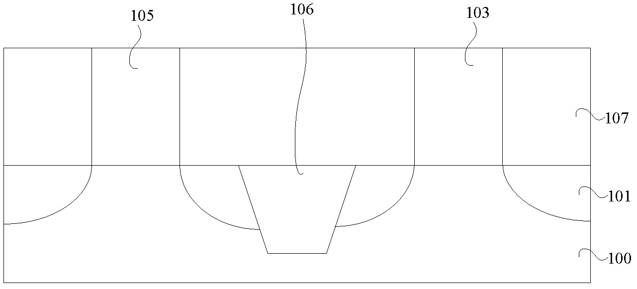
[0031] Step S01: providing a semiconductor substrate, on which an interlayer dielectric layer and a...


PUM


Abstract

The invention discloses a manufacture method of a metal grid of a transistor of a complementary metal-oxide-semiconductor (CMOS). A plurality of patterned photoresist layers are utilized to firstly remove a first nominal grid to form a first grid groove, a first work function metal layer and a first filling layer, and then to remove a second nominal grid to from a second grid groove, a second work function metal layer and a second filling layer. Meanwhile, the first filling layer and the second filling layer are removed to expose the first grid groove and the second grid groove, then a metal grid layer is filled, and a chemical mechanical polishing process is conducted for one time, namely a first metal grid and a second metal grid are formed at the same time. Compared with a method that two chemical mechanical polishing processes need to be adopted to form two metal grids in the process of manufacturing the metal grid of the transistor of the CMOS in the prior art, the manufacture method of the metal grid of the transistor of the CMOS can greatly simplify the process, further reduce polished residues in the chemical mechanical polishing process, reduce the polishing damage to interlayer dielectric layers, and then improve the performance of the transistor of the CMOS.

Description

technical field [0001] The invention relates to a method for manufacturing a semiconductor device, in particular to a method for manufacturing a metal gate of a CMOS transistor. Background technique [0002] As the integration of semiconductor devices becomes higher and higher, the voltage and current required for the operation of semiconductor devices continue to decrease, and the switching speed of transistors is also accelerated, and the requirements for various aspects of semiconductor technology have been greatly increased. The prior art process has made transistors and other types of semiconductor device components as thick as several molecules and atoms, and the materials that make up semiconductors have reached the limit of physical and electrical characteristics. [0003] Then the gate process has entered a new stage. The earliest part to reach the limit is the gate oxide layer of the semiconductor device, also known as the gate dielectric layer. The existing proces...

Claims


Application Information

Patent Timeline
Patent Type & Authority Applications(China)
IPC IPC(8): H01L21/8238H01L21/28
Inventor 王新鹏张海洋
Owner SEMICON MFG INT (SHANGHAI) CORP
Features
  • R&D
  • Intellectual Property
  • Life Sciences
  • Materials
  • Tech Scout
  • Unparalleled Data Quality
  • Higher Quality Content
  • 60% Fewer Hallucinations
Learn More