Crystal Growth Furnace

A technology of crystal growth furnace and reaction chamber, which is applied in the direction of crystal growth, single crystal growth, and from chemically reactive gases. It can solve the problems of high background carrier concentration, adverse effects, and insufficient purity of the reaction chamber. Guaranteed high purity, reduced background carrier concentration, and easy replacement

Active Publication Date: 2016-07-06
SUZHOU INST OF NANO TECH & NANO BIONICS CHINESE ACEDEMY OF SCI
View PDF8 Cites 0 Cited by
  • Summary
  • Abstract
  • Description
  • Claims
  • Application Information

AI Technical Summary

Problems solved by technology

Therefore, silicon carbide epitaxial equipment using graphite felt has the problem that the reaction chamber is not pure enough, which leads to a high background carrier concentration of the epitaxial wafer (generally at 5í10 15 cm -3 above)
Impurities in epitaxial wafers will have adverse effects on the performance of silicon carbide devices such as leakage

Method used


Image

  • Crystal Growth Furnace
  • Crystal Growth Furnace
  • Crystal Growth Furnace

Examples


Embodiment Construction

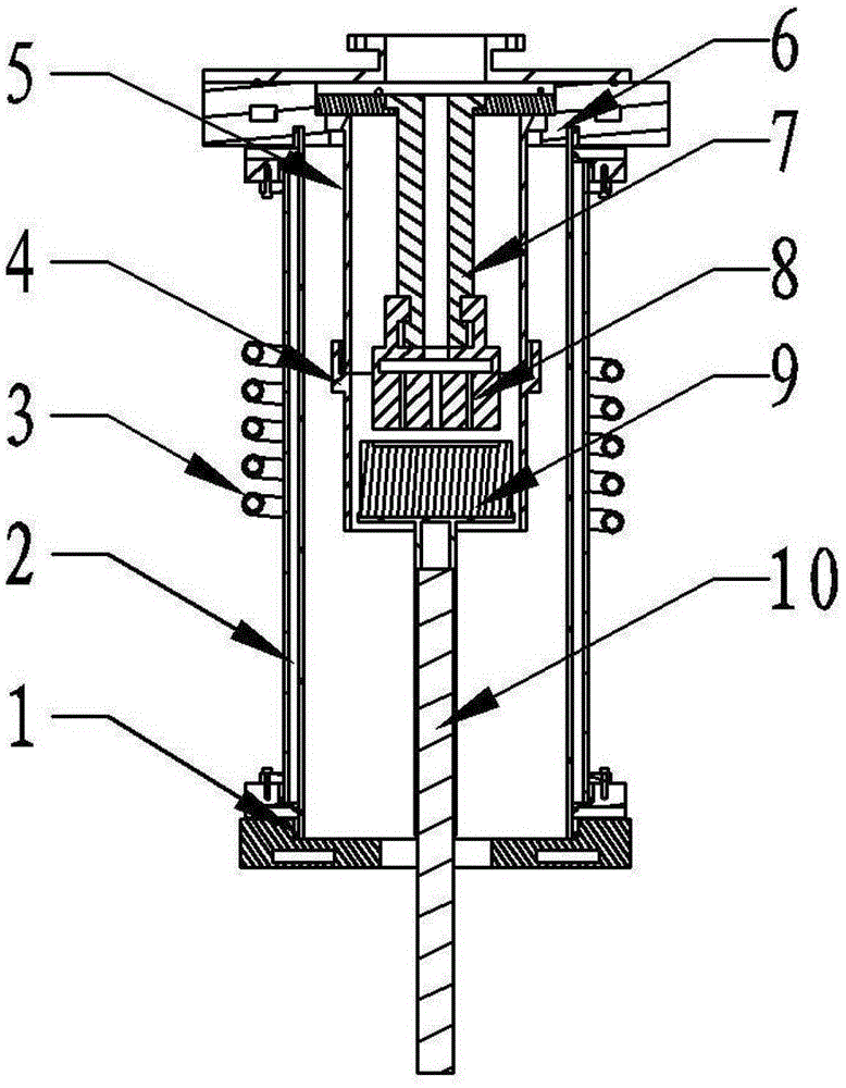
[0023] The purpose of the present invention is to design a high-temperature silicon carbide crystal growth device without graphite felt, which not only improves the cleanliness of the system, reduces the background carrier concentration of the epitaxial wafer, but also meets the needs of high-temperature heating of silicon carbide, thereby obtaining High quality silicon carbide epitaxial wafers.

[0024] Such as figure 1 As shown, the crystal growth furnace provided by the present invention includes: a reaction chamber and a heating device, the reaction chamber includes a first thermal wall 5 and a second thermal wall 4, and the first thermal wall 5 and the second thermal wall 4 are detachably connected, and the first thermal wall 5 and the second thermal wall 4 enclose the reaction space of the crystal, the material of the second thermal wall 4 is graphite, and the heating device 3 cooperates with the second thermal The wall 4 is arranged to heat it; the material of the firs...


PUM


Abstract

The invention discloses a crystal growing furnace which comprises a reaction chamber and a heating device. The reaction chamber comprises a first heat wall and a second heat wall. The first and second heat walls are detachably connected and define a reaction space for crystals. The second heat wall is made of graphite. The heating device is matched with the second heat wall to heat the second heat wall. The first heat wall is made of a high temperature heat-resisting material. In the device, no graphite felts are used for insulation of the reaction chamber, so that the problem of impurity pollution in the reaction chamber caused by using the graphite felts is eliminated, and the background carrier concentration of an epitaxial wafer is greatly reduced. Furthermore, the detachable heat walls adopted are easy to install and convenient to change.

Description

technical field [0001] The invention relates to the field of crystal growth, in particular to a crystal growth device for epitaxial growth of silicon carbide. Background technique [0002] Silicon carbide (SiC) is a third-generation wide bandgap semiconductor material with wide bandgap, high breakdown voltage, high thermal conductivity, high electron saturation drift rate, high electron mobility, small dielectric constant, strong radiation resistance, High chemical stability and other advantages are the key materials for manufacturing high temperature, high frequency, high power, radiation resistance, non-volatile storage devices and optoelectronic integrated devices. Silicon carbide power electronic devices have the characteristics of high conversion efficiency, high temperature resistance, and radiation resistance. They have gradually replaced silicon devices in the fields of power conversion, solar photovoltaics, electric vehicles, and high-efficiency motors, and have beg...

Claims


Application Information

Patent Timeline
Patent Type & Authority Patents(China)
IPC IPC(8): C30B25/02C30B25/08
Inventor 王劼张立国范亚明张洪泽
Owner SUZHOU INST OF NANO TECH & NANO BIONICS CHINESE ACEDEMY OF SCI
Why Eureka
Try Eureka