Full-solution-processed multilayered-structure transparent conductive thin film and preparation method thereof

A transparent conductive film, multi-layer structure technology, applied in cable/conductor manufacturing, conductive layer on insulating carrier, circuit, etc., can solve problems such as poor stability, unengineered, poor adhesion, etc., to achieve environmental stability High performance, excellent electrical performance and simple operation

Active Publication Date: 2013-07-10
CHANGCHUN INST OF OPTICS FINE MECHANICS & PHYSICS CHINESE ACAD OF SCI
View PDF3 Cites 22 Cited by
  • Summary
  • Abstract
  • Description
  • Claims
  • Application Information

AI Technical Summary

Problems solved by technology

[0005] In order to solve the problem that the single-layer structure metal nanowire transparent conductive film has large roughness, poor adhesion and poor stability in the prior art, and the preparation method of the multi-layer structure transparent conductive film is not conducive to the preparation of large-area flexible transparent conductive film, it is impossible to The technical problem of engineering, the present invention provides a kind of whole solution processing multi-layer structure transparent conductive film and its preparation method

Method used


Image

  • Full-solution-processed multilayered-structure transparent conductive thin film and preparation method thereof
  • Full-solution-processed multilayered-structure transparent conductive thin film and preparation method thereof
  • Full-solution-processed multilayered-structure transparent conductive thin film and preparation method thereof

Examples


preparation example Construction

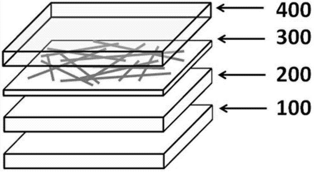
[0058] The preparation method of the full-solution processing multilayer structure transparent conductive film comprises the following steps:

[0059] (1) Prepare the first dielectric reinforcement layer 200 on the planar substrate 100 by using a solution processing method;

[0060] (2) Prepare the metal nanowire layer 300 on the first dielectric reinforcement layer 200 by using a solution processing method;

[0061] (3) Prepare a second dielectric protection layer 400 on the metal nanowire layer 300 by using a solution processing method;

[0062] The first dielectric reinforcement layer 200 is made of any metal oxide semiconductor sol or a mixture of any multiple metal oxide semiconductor sols;

[0063] The second dielectric protection layer 400 is made of any metal oxide semiconductor sol or a mixture of any multiple metal oxide semiconductor sols;

[0064] The metal nanowire layer 300 is made of a metal nanowire solution.

[0065] In the embodiment of the present inventi...

Embodiment 1

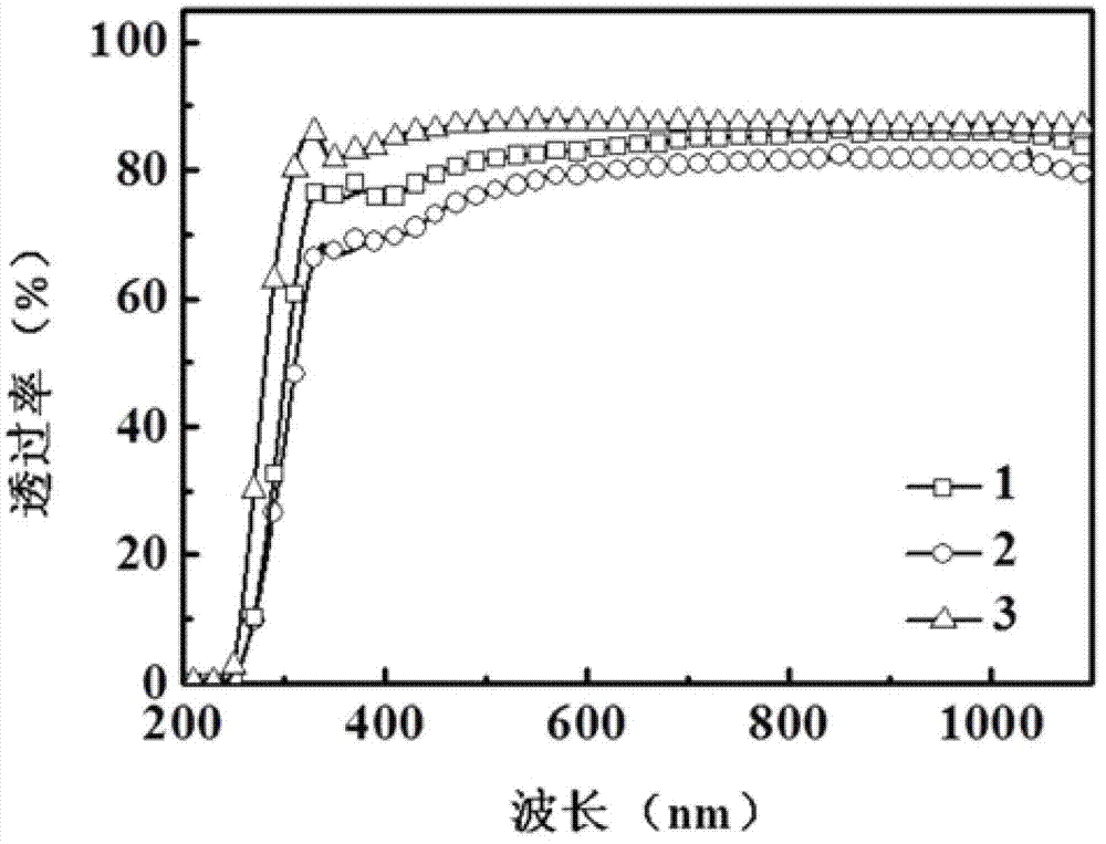
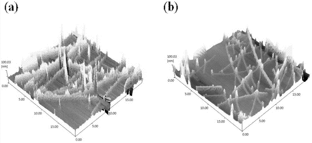
[0092] combine figure 2 , image 3 and Figure 4 Illustrative Example 1

[0093] Preparation of TiOx / AgNW / TiOx multilayer transparent conductive film:

[0094]After the planar substrate 100 was cleaned and dried, TiOx with a thickness of 10 nm was used as the first dielectric reinforcement layer 200, AgNW with a thickness of 70 nm as the metal nanowire layer 300 and a thickness of 10nm of TiOx is used as the second dielectric protection layer 400 to finally form a multi-layer transparent conductive film with the structure of TiOx (10nm) / AgNW (70nm) / TiOx (10nm). Wherein the planar substrate 100 is a glass substrate; the first dielectric reinforcement layer 200 and the second dielectric protection layer 400 are prepared by a spin coating method; the metal nanowire layer 300 is prepared by a drop coating method, and the AgNW has a diameter of 50 nm and a length of 15 μm. The concentration of AgNW solution is 0.2 mg / ml.

[0095] The visible light average transmittance, surfa...

Embodiment 2

[0099] to combine figure 2 and Figure 4 Illustrative Example 2

[0100] V 2 o 5 / AgNW / V 2 o 5 Preparation of a multilayer structured transparent conductive film:

[0101] After cleaning and drying the planar substrate 100, use V 2 o 5 Sol and ethanol-dispersed AgNW solution were sequentially prepared into V with a thickness of 30 nm 2 o 5 As the first dielectric reinforcement layer 200, AgNW with a thickness of 70 nm as the metal nanowire layer 300 and V with a thickness of 40 nm 2 o 5 As the second dielectric protection layer 400, the final structure is V 2 o 5 (30nm) / AgNW(70nm) / V 2 o 5 (40nm) multilayer structure transparent conductive film. Wherein the planar substrate 100 is a glass substrate; the first dielectric reinforcement layer 200 and the second dielectric protection layer 400 are prepared by a spin coating method; the metal nanowire layer 300 is prepared by a drop coating method, and the AgNW has a diameter of 50 nm and a length of 15 μm. The conc...


PUM

PropertyMeasurementUnit
thicknessaaaaaaaaaa
thicknessaaaaaaaaaa
diameteraaaaaaaaaa

Abstract

The invention provides a full-solution-processed multilayered-structure transparent conductive thin film and a preparation method of the full-solution-processed multilayered-structure transparent conductive thin film, belongs to the technical field of conductive thin film materials, and solves technical problems that in the prior art, a single-layer-structure metal nanowire transparent conductive thin film is high in roughness, small in adhesive force and poor in stability, a preparation method of a multilayered-structure transparent conductive thin film is not in favor of preparing a large-area flexible transparent conductive thin film and cannot be engineered. According to the preparation method of the full-solution-processed multilayered-structure transparent conductive thin film, metal oxide semiconductor sols are used as raw materials of a dielectric layer, metal nanowires dispersed by organic solvents are used as raw materials of a metal layer, and the multilayered-structure transparent conductive thin film is prepared with adoption of a solution processing method. The preparation method of the full-solution-processed multilayered-structure transparent conductive thin film achieves large-area flexible production of the multilayered-structure transparent conductive thin film, and the prepared transparent conductive thin film is strong in adhesive force, high in visible light average transmittance (81.5%), low in surface roughness (2.1nm), high in environmental stability, and outstanding in photoelectric performance.

Description

technical field [0001] The invention relates to a fully solution processed multilayer transparent conductive film and a preparation method thereof, belonging to the technical field of conductive film materials. technical background [0002] Transparent conductive film is an important optoelectronic functional film, which is widely used in optoelectronic devices such as liquid crystal display, organic light emitting diode, touch screen and thin film solar cell. The future development trend of optoelectronic devices is high performance, low cost, flexibility and light weight, so higher requirements are put forward for the transparent conductive films used in them. The most commonly used and commercialized transparent conductive film is indium tin oxide (ITO) film, which has high visible light transmittance and low resistivity, and is often used in organic solar cells and organic light-emitting diodes. And other optoelectronic devices as transparent electrodes. However, the s...

Claims


Application Information

Patent Timeline
Patent Type & Authority Applications(China)
IPC IPC(8): H01B5/14H01B13/00
Inventor 郭晓阳刘星元
Owner CHANGCHUN INST OF OPTICS FINE MECHANICS & PHYSICS CHINESE ACAD OF SCI
Why Eureka
Try Eureka