

Cleaning process method of crystal silicon slice
A process method and technology for crystalline silicon wafers, which are applied in the directions of cleaning methods using liquids, cleaning methods and utensils, chemical instruments and methods, etc. Improve productivity and increase the effect of backside polishing
- Summary
- Abstract
- Description
- Claims
- Application Information
AI Technical Summary
Problems solved by technology
Method used
Image

Examples
Embodiment Construction
[0034] The invention will be described in detail below in conjunction with the accompanying drawings and embodiments.
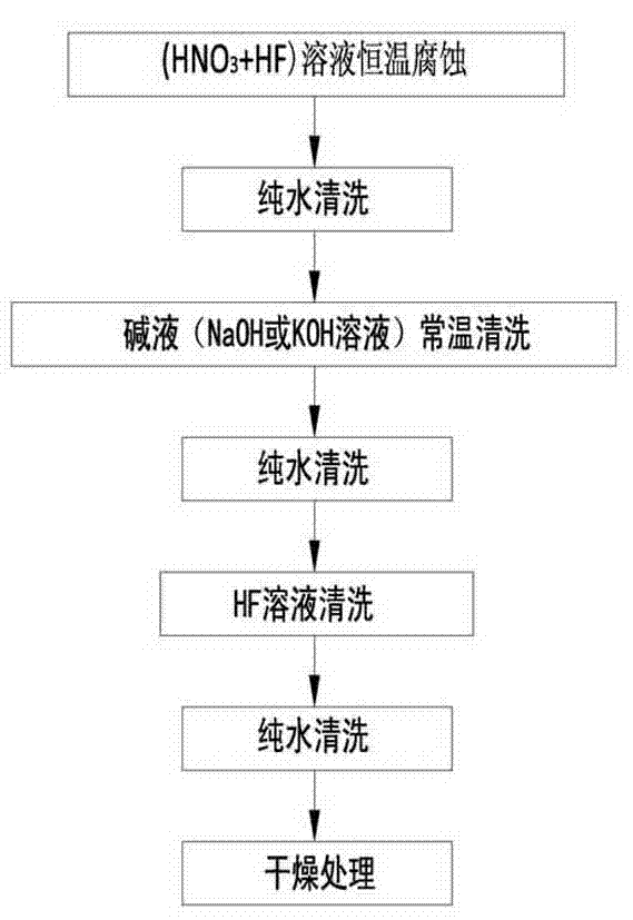
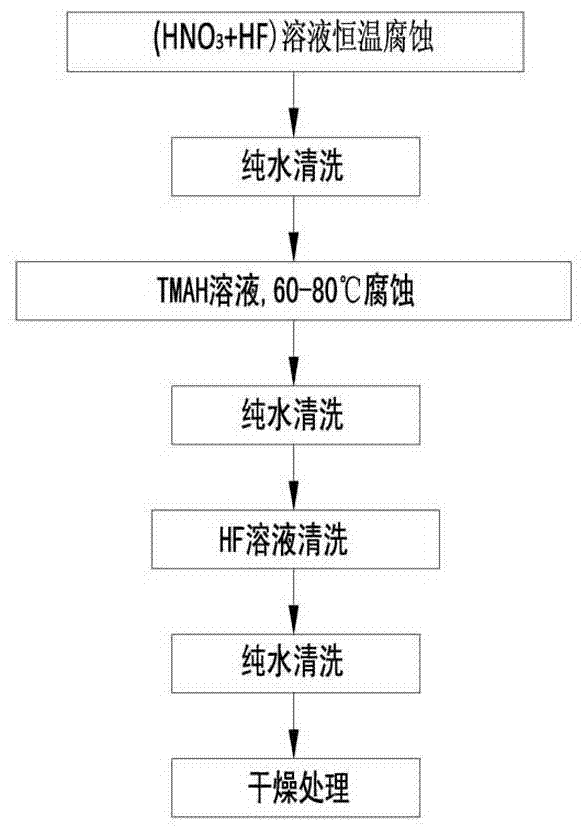
[0035] Such as figure 2 Shown, the cleaning process method of the crystalline silicon wafer that the present invention proposes comprises the following steps:
[0036] Step 1. First place the silicon wafer in HF with a temperature controlled at 8-16°C and a volume concentration of 5-7.5%.
[0037] 35-45% HNO 3 Soak in the mixed solution for 0.8-1.5 minutes, and carry out acid etching treatment, so as to achieve the purpose of etching the back and surrounding of the silicon wafer. In this process, according to the consumption of the reaction between the solution and the silicon wafer, a certain amount of HF and HNO is timely added 3 , to ensure the proper ratio of the solution.
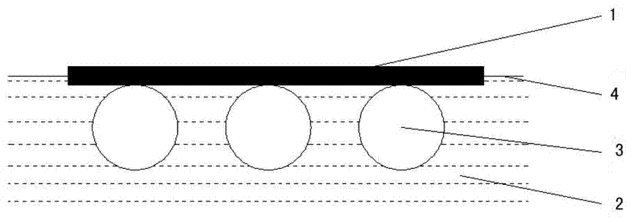
[0038] image 3 is a schematic diagram of step 1. In step 1, wafer 1 is placed on HNO 3 On the driving roller shaft 3 provided in the HF mixed solution 2, the liquid level 4 o...
PUM
 Abstract
Description
Claims
Application Information