Mask plate for vapor plating

A mask and evaporation technology, applied in vacuum evaporation plating, sputtering plating, ion implantation plating, etc., can solve the problem of inability to reach the substrate, improve service life, improve uniformity, and avoid board surface deformation Effect

Inactive Publication Date: 2013-07-17
KUN SHAN POWER STENCIL
View PDF5 Cites 1 Cited by
  • Summary
  • Abstract
  • Description
  • Claims
  • Application Information

AI Technical Summary

Problems solved by technology

[0014] The technical problem to be solved by the present invention is that in the existing OLED manufacturing technology, the organic particles cannot reach the substrate due to the shielding of the opening wall during evaporation. A new mask for evaporation is provided, which has organic The advantages of high material utilization rate, high film formation rate, long service life of mask plate and cost saving

Method used


Image

  • Mask plate for vapor plating
  • Mask plate for vapor plating
  • Mask plate for vapor plating

Examples


Embodiment 1

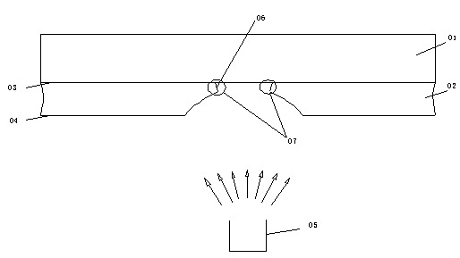
[0031] A mask plate for evaporation, which is a quadrilateral stainless steel metal plate, the mask plate has a two-layer structure of an ITO surface layer and an evaporation surface layer, and the mask plate has an opening through the ITO surface layer and the evaporation surface layer , the opening size of the ITO surface layer is smaller than the opening size of the evaporation surface layer, and the shape of the opening is an isosceles trapezoid in the transverse section along the thickness direction of the mask plate. Such as figure 2 shown.

[0032]A mask for evaporation with a thickness of 20 μm is prepared by electroforming, and it is covered with openings. The uniformity of the mask is less than 5%, the surface brightness is first-class brightness, and the lateral dimension of the opening on the ITO surface layer is 20 μm, and The dimensional accuracy is ±5μm, but the opening size increases from the ITO surface layer to the evaporation surface layer, and the opening...

Embodiment 2

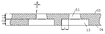
[0035] A mask plate for evaporation, which is a rectangular Invar metal plate, the mask plate has a two-layer structure of an ITO surface layer and an evaporation surface layer, and the mask plate has a penetrating ITO surface layer and an evaporation surface layer. The opening of the layer, the opening size of the ITO surface layer is smaller than the opening size of the evaporation surface layer, and the shape of the opening is trapezoidal on the transverse section along the thickness direction of the mask plate.

[0036] A mask for evaporation with a thickness of 20 μm was prepared by electroforming, which is covered with openings. The uniformity of the mask is less than 5%, the surface brightness is first-class brightness, the size of the opening on the ITO surface is 10 μm, and the dimensional accuracy is in ±5μm, but the size of the opening increases from the ITO surface to the evaporation surface. Cut the opening vertically along the thickness direction of the mask to ob...

Embodiment 3

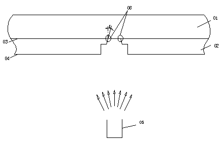
[0040] A mask for evaporation is shaped as a rectangular nickel-cobalt alloy metal plate. The mask has a two-layer structure of an ITO surface layer and an evaporation surface layer. The opening, the opening size of the ITO surface layer is smaller than the opening size of the evaporation surface layer, and the shape of the opening is trapezoidal on the transverse section along the thickness direction of the mask plate.

[0041] The thickness of the ITO surface layer is 20um, and the thickness of the evaporated surface layer is 80um. The openings on the ITO surface and the evaporation surface are connected by several solid bridges, and the openings are regularly distributed on the mask; The direction of the dimension side is transverse, and the transverse dimension of the opening on the ITO surface is smaller than the transverse dimension of the opening on the evaporation surface. The lateral dimensional accuracy of the opening on the ITO surface is ±5 μm; the vertical depth ...


PUM

PropertyMeasurementUnit
thicknessaaaaaaaaaa
thicknessaaaaaaaaaa
thicknessaaaaaaaaaa

Abstract

The invention relates to a mask plate for vapor plating, and aims to mainly solve the technical problem that organic particles cannot reach a substrate due to shadowing of a mask plate aperture wall during vapor plating in the existing OLED (organic light-emitting diode) manufacturing technologies. The mask plate for vapor plating adopted in the invention is a quadrilateral metal plate, which comprises an ITO (indium tin oxide) surface layer and a vapor plating surface layer in structure. The mask plate is equipped with apertures running through the ITO surface layer and the vapor plating surface layer. The aperture size of the ITO surface layer is smaller than that of the vapor plating surface layer. And the apertures on the cross section of the mask plate in the thickness direction are in a trapezoid shape. According to the technical scheme, the problem is well solved. Thus, the mask plate for vapor plating can be used in the industrial production of organic light-emitting diodes.

Description

[0001] technical field [0002] The invention relates to a mask plate for vapor deposition required in the OLED manufacturing process. Background technique [0003] Generally, an OLED device is an emissive display device that emits light by electrically exciting a fluorescent organic compound. The OLED device can be regarded as a passive matrix OLED (PMOLED) device or an active matrix OLED (AMOLED) device according to a driving manner of N×M pixels that can be arranged in a matrix. Compared with PMOLED devices, AMOLED devices are suitable for large-sized displays due to their low power consumption and high resolution. [0004] Depending on the direction in which light is emitted from the organic compound, the OLED device can be a top-emitting OLED device, a bottom-emitting OLED device, or a top and bottom-emitting OLED device. Top-emitting OLED devices emit light in the opposite direction to the substrate on which the pixels are disposed and, unlike bottom-emitting OLEDs, ...

Claims


Application Information

Patent Timeline
Patent Type & Authority Applications(China)
IPC IPC(8): C23C14/04C23C14/24
Inventor 魏志凌高小平
Owner KUN SHAN POWER STENCIL
Why Eureka
Try Eureka