nldmos structure compatible with 5 volt cmos process and its fabrication method

A kind of process, N-type technology, applied in the field of NLDMOS structure and its manufacturing method, can solve the problems such as inability to share, and achieve the effect of a large safe working area

Active Publication Date: 2015-12-09
SHANGHAI HUAHONG GRACE SEMICON MFG CORP
View PDF5 Cites 0 Cited by
  • Summary
  • Abstract
  • Description
  • Claims
  • Application Information

AI Technical Summary

Problems solved by technology

In the BCD (Bipolar-CMOS-DMOS) process, although DMOS and CMOS are integrated in the same chip, due to the requirements of high withstand voltage and low on-resistance, the conditions of the background area and drift area of ​​DMOS are often not comparable to those of CMOS. Existing process conditions sharing

Method used


Image

  • nldmos structure compatible with 5 volt cmos process and its fabrication method
  • nldmos structure compatible with 5 volt cmos process and its fabrication method
  • nldmos structure compatible with 5 volt cmos process and its fabrication method

Examples


Embodiment Construction

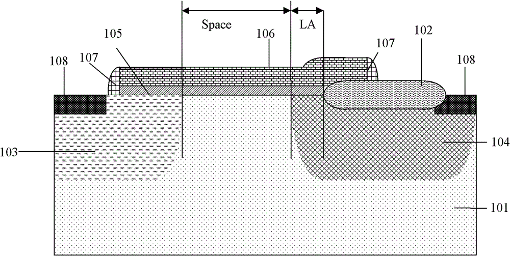
[0039] The NLDMOS structure compatible with the 5-volt CMOS process of the present invention, such as figure 1 As shown, it includes: a field oxygen region 102, a polysilicon gate 106, a gate oxide layer 105, an isolation spacer 107, and a source and drain 108 formed compatible with a 5-volt CMOS process, and a P-type notebook composed of a P well 103 in a CMOS process. The bottom region is an N-type drift region composed of an N well 104 in a CMOS process; wherein, the P-type background region and the N-type drift region are located in the P-type substrate 101, and the P-type background region and the N-type drift region The distance (Space) between them is 0.5-2 μm; the source and drain 108 are located in the P-type background region and the N-type drift region; the gate oxide layer 105 is located on the upper surface of the P-type substrate 101; the polysilicon gate 106 is located in the gate oxide layer 105; the isolation spacer 107 is adjacent to the polysilicon gate 106;...


PUM


Abstract

The invention discloses an N-type laterally diffused metal oxide semiconductor (NLMOS) structure compatible with a 5-V complementary metal oxide semiconductor (CMOS) process and a manufacturing method thereof. The structure comprises a field oxygen area, a polycrystalline silicon grid, a grid oxidizing layer, an isolation lateral wall and a source drain, wherein the field oxygen area, the polycrystalline silicon grid, the grid oxidizing layer, the isolation lateral wall and the source drain are formed through the 5-V CMOS process in compatible mode. The structure further comprises a P-type base area formed by a P trap in the CMOS process and an N drifting area formed by an N trap in the CMOS process. The manufacturing method includes: 1) using the P trap as the P-type base area and the N trap as the N drifting area; 2) controlling the distance between the P-type base area and the N drifting area; 3) shortening the length of an accumulation area to -0.2-0.1mum; and 4) finishing manufacturing of the field oxygen area, the polycrystalline silicon grid, the grid oxidizing layer, the isolation lateral wall, the source drain and electrodes in connection mode according to the 5-V CMOS process. By means of the structure and the method, breakdown voltage can reach over 25V, and use requirements of switching devices and simulation devices can be met.

Description

technical field [0001] The invention relates to an NLDMOS (N-type lateral double-diffused metal oxide semiconductor) structure and a manufacturing method thereof, in particular to an NLDMOS structure compatible with a 5-volt CMOS (complementary metal oxide semiconductor) process and a manufacturing method thereof. Background technique [0002] DMOS (Double Diffused Metal Oxide Semiconductor) is currently widely used in power management circuits due to its high voltage resistance, high current drive capability and extremely low power consumption. In the BCD (Bipolar-CMOS-DMOS) process, although DMOS and CMOS are integrated in the same chip, due to the requirements of high withstand voltage and low on-resistance, the conditions of the background area and drift area of ​​DMOS are often not comparable to those of CMOS. Existing process conditions are shared. The main reason is that in the case of high withstand voltage, DMOS needs the doping of the drift region to be light, so ...

Claims


Application Information

Patent Timeline
Patent Type & Authority Patents(China)
IPC IPC(8): H01L29/78H01L29/06H01L21/336
CPCH01L29/1045H01L29/42368H01L29/7835
Inventor 石晶刘冬华段文婷胡君
Owner SHANGHAI HUAHONG GRACE SEMICON MFG CORP
Why Eureka
Try Eureka