Solar cell manufacturing method and solar cell

A technology of solar cells and manufacturing methods, which is applied to circuits, photovoltaic power generation, electrical components, etc., can solve the problems of inability to accurately control doping ion concentration and doping uniformity, and high manufacturing costs, and achieve cost reduction and simplification of process steps Effect

Inactive Publication Date: 2013-07-17
KINGSTONE SEMICONDUCTOR LIMITED COMPANY
View PDF6 Cites 12 Cited by
  • Summary
  • Abstract
  • Description
  • Claims
  • Application Information

AI Technical Summary

Problems solved by technology

[0005] The technical problem to be solved by the present invention is to overcome the defect that the production of IBC solar cells in the prior art requires the use of photolithography, high production costs, and the inability to accurately control the concentration of doping ions and the uniformity of doping in the doping process of thermal diffusion. , to provide a solar cell manufacturing method and a solar cell with few process steps, no need for a photolithography machine, low cost, precise control of doping uniformity and dopant dosage, and high photoelectric conversion efficiency

Method used


Image

  • Solar cell manufacturing method and solar cell
  • Solar cell manufacturing method and solar cell
  • Solar cell manufacturing method and solar cell

Examples


Embodiment 1

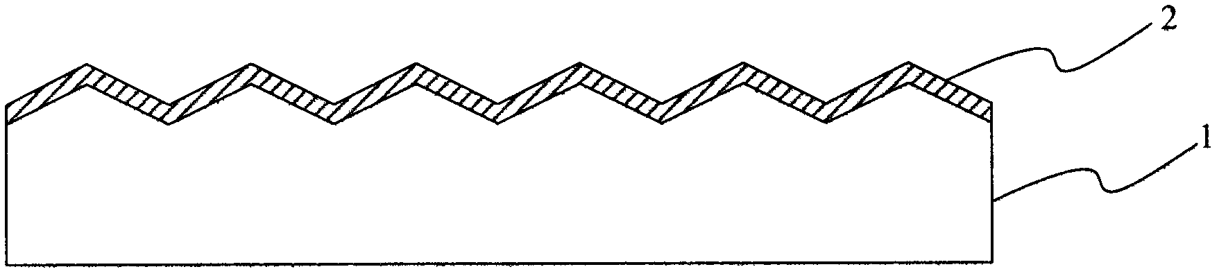
[0069] refer to figure 1 , forming a surface N+ doped layer 2 on the surface of the N-type substrate 1 , specifically, forming the surface N+ doped layer 2 by thermal diffusion. Wherein, the surface of the N-type substrate 1 is suede to increase the utilization rate of sunlight.

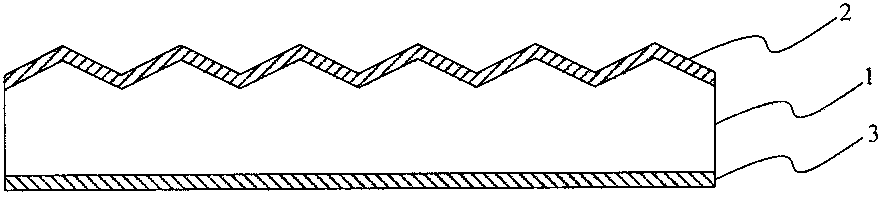
[0070] refer to figure 2 , forming an N+ doped layer 3 in the back of an N-type base 1, wherein the N+ doped layer 3 is formed by thermal diffusion. In this embodiment, BBr 3 As a diffusion source, the N+ doped layer 3 is BSG (borosilicate glass).

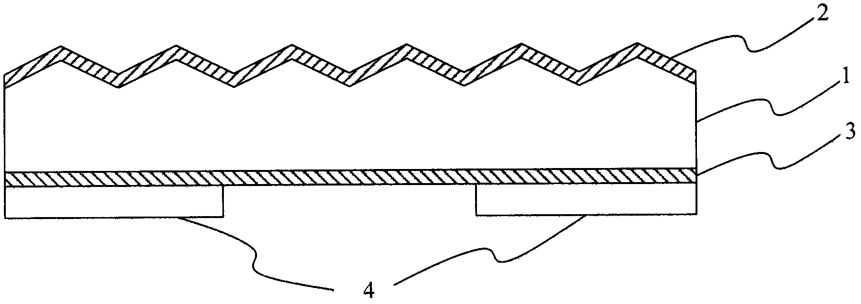
[0071] refer to image 3 A mask 4 is formed on the N+ doped layer 3 by screen printing, wherein the area not covered by the mask 4 is an open area. Wherein, the mask has a thickness of 10 μm and is made of photoresist.

[0072] refer to Figure 4 Etching the N+ doped layer 3 in the open area to the N-type substrate 1 by wet chemical method, and forming an undercut 41 in the N+ doped layer 3 above the mask 4 close to one end of the open area, where...

Embodiment 2

[0080] The principle and steps of embodiment 2 are all the same as embodiment 1, the only difference is:

[0081] refer to image 3 , the thickness of the mask is 40 μm.

[0082] refer to Figure 4 , the depth w of the formed side erosion 1 is 5 μm, and the depth of the etched N-type substrate is 3 μm.

[0083] refer to Figure 5 Accelerating boron ions to 50keV and implanting the boron ions from the open area on the surface of the N-type substrate into the N-type substrate 1 by ion implantation to form a P+ doped region 5 with a sheet resistance of 200Ω / □.

[0084] refer to Figure 9and forming a first metal layer on the second passivation layer by using metal nickel to fill the first type contact hole and the second type contact hole with the metal nickel, and sintering the first metal layer. Afterwards, a second metal layer is formed on the first metal layer by using metallic copper. In this embodiment, the stack of the first metal layer and the second metal layer is ...

Embodiment 3

[0088] The principle and steps of embodiment 3 are all the same as embodiment 1, the only difference is:

[0089] refer to Figure 4 , the depth w of the formed side erosion 1 is 3 μm, and the depth of the etched N-type substrate is three times the thickness of the N+ doped layer 3 .

[0090] refer to Figure 5 Accelerating boron ions to 30keV and implanting the boron ions from the open area on the surface of the N-type substrate into the N-type substrate 1 by ion implantation to form a P+ doped region 5 with a sheet resistance of 100Ω / □.

[0091] All the other unmentioned parts are the same as in Example 1.


PUM

PropertyMeasurementUnit
thicknessaaaaaaaaaa
thicknessaaaaaaaaaa
thicknessaaaaaaaaaa

Abstract

The invention discloses a solar cell manufacturing method. The solar cell manufacturing method includes that a PN structure is obtained; a first passivation layer and an antireflection layer are formed on the surface of a substrate material of the PN structure, and a second passivation layer is formed on the back of the substrate material of the PN structure; a first kind of contact holes and a second kind of contact holes are formed; a first metal layer is formed on the second passivation layer so as to enable the first kind of contact holes and the second kind of contact holes to be filled by first metal; a second metal layer is formed on the first metal layer; the first metal layer and the second metal layer which are stacked are divided into a first kind of electrodes and a second kind of electrodes, wherein the first kind of electrodes are connected to P+ doped regions through the first metal in the first kind of contact holes, and the second kind of electrodes are connected to N+ doped regions through the first metal in the second kind of contact holes. A solar cell is further disclosed. By means of the method and the solar cell, process steps are simplified, a mask is adopted only once, and the cost is greatly reduced.

Description

technical field [0001] The invention relates to a method for manufacturing a solar cell and a solar cell, in particular to a method for manufacturing a back-contact solar cell and the back-contact solar cell. Background technique [0002] New energy is one of the five most decisive technological fields in the world economic development in the 21st century. Solar energy is a clean, efficient and inexhaustible new energy source. In the new century, the governments of various countries regard the utilization of solar energy resources as an important content of the national sustainable development strategy. Photovoltaic power generation has the advantages of safety, reliability, no noise, no pollution, less constraints, low failure rate, and easy maintenance. [0003] In recent years, with the rapid development of international photovoltaic power generation, the supply of solar chips is in short supply, so improving the photoelectric conversion efficiency of solar chips and th...

Claims


Application Information

Patent Timeline
Patent Type & Authority Applications(China)
IPC IPC(8): H01L31/18H01L31/068H01L31/0352
CPCY02E10/547Y02P70/50
Inventor 陈炯洪俊华钱锋
Owner KINGSTONE SEMICONDUCTOR LIMITED COMPANY
Why Eureka
Try Eureka