A trench gate type igbt with double-sided diffusion residual layer and its manufacturing method

A technology of diffusion residual layer and double-sided diffusion, which is applied in semiconductor/solid-state device manufacturing, electrical components, circuits, etc., can solve the problems of rising manufacturing costs of process steps, achieve good controllability and stability, improve current capability, current The effect of increasing ability

Inactive Publication Date: 2016-04-13
ZHEJIANG UNIV +1
View PDF4 Cites 0 Cited by
  • Summary
  • Abstract
  • Description
  • Claims
  • Application Information

AI Technical Summary

Problems solved by technology

However, both the carrier storage layer and the planar enhancement layer are formed by adding additional process steps when forming the front MOSFET structure during the IGBT manufacturing process. The increase in the process steps will inevitably increase the manufacturing cost.

Method used


Image

  • A trench gate type igbt with double-sided diffusion residual layer and its manufacturing method
  • A trench gate type igbt with double-sided diffusion residual layer and its manufacturing method
  • A trench gate type igbt with double-sided diffusion residual layer and its manufacturing method

Examples


Embodiment Construction

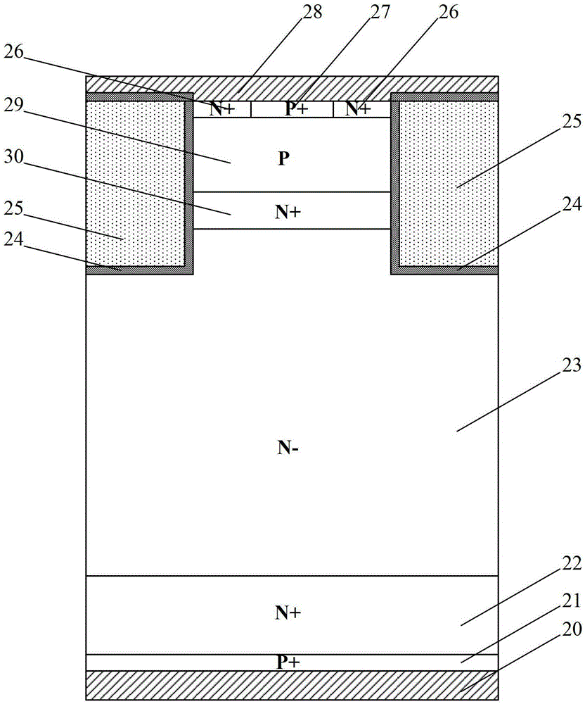
[0032] Such as figure 1 As shown, a trench gate type IGBT with a double-sided diffused residual layer includes an N-type base region, a P-type base region 29, a back P+ collector region 21, an N+ emitter region 26, a P+ emitter region 27, Gate oxide layer 24, emitter 28, gate electrode 25 and collector 20, wherein the N-type base region is composed of N+ diffusion residual layer 30, N-drift region 23 and N+ buffer layer 22 in sequence. The IGBT manufacturing process is shown in Figure 2 As shown, the details are as follows:

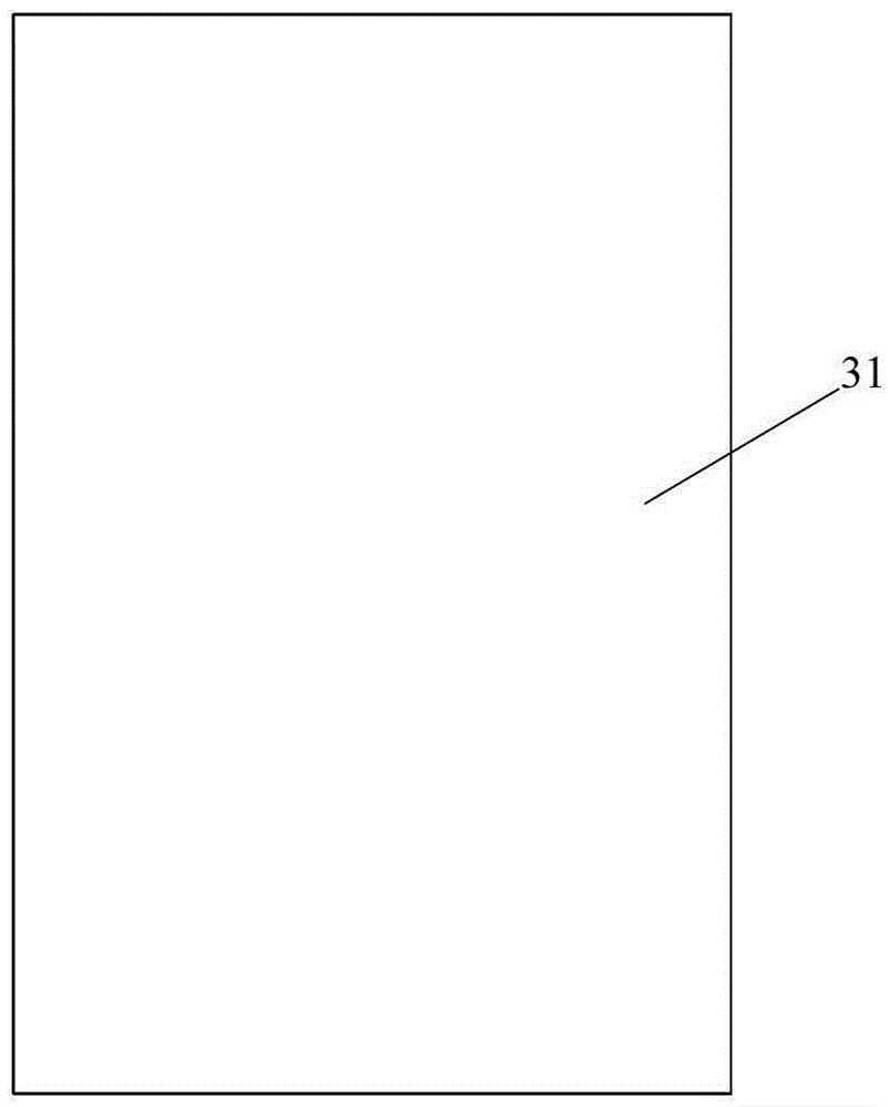
[0033] Such as Figure 2a The shown N-type single crystal substrate 31 with a crystal orientation of has a doping concentration of 4.3×10 13 cm -3 , the thickness is 500um, according to the needs of the forward blocking voltage (such as 1700V, the same below), the doping concentration can be adjusted to 1×10 13 ~2×10 14 cm -3 .

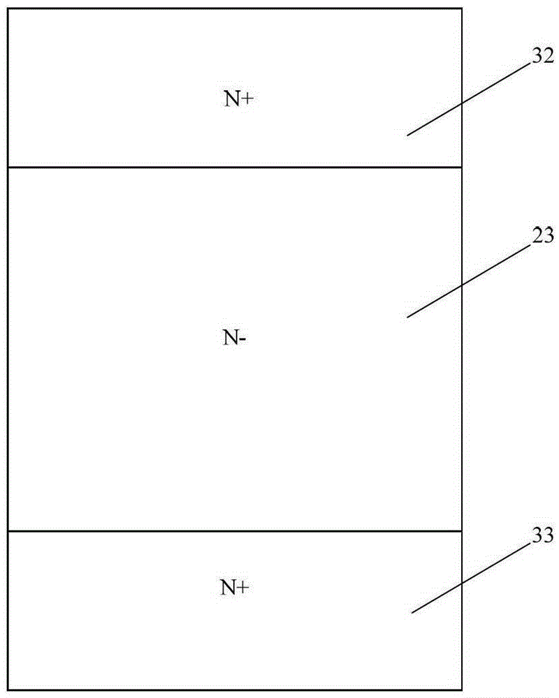
[0034] Such as Figure 2b As shown, the N-type single crystal substrate undergoes a double-sided high-temperature deep...


PUM


Abstract

The invention discloses a trench gate type insulated gate bipolar translator (IGBT) with a double-face diffusion residual layer and a manufacturing method thereof. The IGBT comprises an N-type base region, a P-type base region, a back P+ collector region, an N+ emitter region, a P+ emitter region, a gate oxide layer, an emitter, a gate electrode and a collector. The N-type base region is composed of an N+ diffusion residual layer, an N- drift region and an N+ buffer layer, wherein the N-type diffusion residual layer, the N- drift region and the N+ buffer layer are stacked up in sequence. The P-type base region is located on the N+ diffusion residual layer. Doping concentration gradually increases outwards from a boundary of the N- drift region with the N+ diffusion residual layer and the N+ buffer layer. The manufacturing method of the IGBT is characterized in that the non-uniform doped N+ layers are formed on the front face and the back face through one-time double-face high temperature deep junction diffusion at the same time, the N+ diffusion residual layer is formed on the front face of the N- drift region, so that the ion doping concentration of the N-type front face is improved, and a conductivity modulation effect is strengthened. The N+ buffer region on the back face can reduce breakover voltage drop of a device, and the turn-off time of the device is prolonged. The manufacturing method can reduce the steps of manufacturing the IGBT, and reduce the cost.

Description

technical field [0001] The invention relates to the field of semiconductor power devices and manufacturing, in particular to a trench gate type IGBT structure with double-sided diffusion residual layers and a manufacturing method thereof. Background technique [0002] IGBT is an insulated gate bipolar transistor (InsulatedGateBipolarTransistor, referred to as IGBT) is a combination of metal oxide semiconductor field effect transistor (MOSFET) gate voltage control characteristics and bipolar junction transistor (BJT) low on-resistance characteristics in All-in-one semiconductor power devices. With the characteristics of voltage control, large input impedance, low driving power, small on-resistance, low switching loss and high operating frequency, it is an ideal semiconductor power switching device with broad development and application prospects. [0003] According to whether there is a high-concentration buffer layer of the same concentration type as the drift region betwee...

Claims


Application Information

Patent Timeline
Patent Type & Authority Patents(China)
IPC IPC(8): H01L29/739H01L21/331
Inventor 张斌韩雁余庆张世峰朱大中
Owner ZHEJIANG UNIV
Why Eureka
Try Eureka