Eureka AIR delivers breakthrough ideas for toughest innovation challenges, trusted by R&D personnel around the world.

Thin film transistor, array substrate, manufacturing method and display device

A technology of thin-film transistors and array substrates, applied in the display field, can solve problems such as poor pixel bright spots, incomplete etching, and lower product quality levels, so as to reduce defective pixels, avoid bridging, and improve product yield.

Active Publication Date: 2013-07-24
HEFEI BOE OPTOELECTRONICS TECH +1
View PDF5 Cites 6 Cited by
  • Summary
  • Abstract
  • Description
  • Claims
  • Application Information

AI Technical Summary

Problems solved by technology

[0006] However, limited by the current process equipment and process capabilities, the channel (the conductive region confined between the source and the drain is called the channel, and the gap between the source and the drain or the trench phase when the gate voltage is turned on The corresponding semiconductor part) is often not completely etched, causing the source and drain to bridge (Bridge), resulting in poor bright spots in the pixel (Pixel), reducing the product quality level (for example: product quality level from P level down to S level)

Method used


Image

  • Thin film transistor, array substrate, manufacturing method and display device
  • Thin film transistor, array substrate, manufacturing method and display device
  • Thin film transistor, array substrate, manufacturing method and display device

Examples


preparation example Construction

[0054] A preparation method of a thin film transistor, comprising the step of forming the source layer and the drain layer on different layers and forming the gate layer and the drain layer on the same layer.

[0055] A method for preparing an array substrate, including the above-mentioned method for preparing a thin film transistor.

Embodiment 1

[0057] A thin film transistor, comprising a substrate and a gate layer, a source layer, and a drain layer arranged on the substrate, the source layer and the drain layer are arranged on different layers, and the drain layer is provided in the same layer as the gate layer.

[0058] An array substrate, including the above-mentioned thin film transistor.

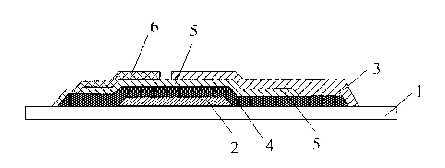
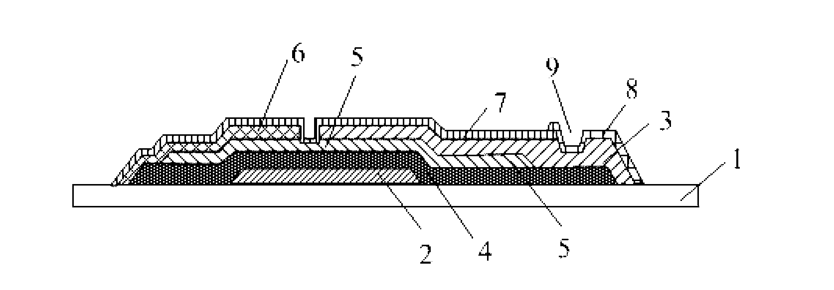
[0059] Such as figure 2 As shown, in the thin film transistor, the drain layer 3 and the gate layer 2 are arranged on the substrate 1 in the same layer, and there is a gap or gap between the drain layer 3 and the gate layer 2 trench; the source layer 6 is disposed above the gate layer 2, and a gate insulating layer 4 and a composite layer 5 are disposed between the source layer 6 and the gate layer 2, and the gate The electrode insulating layer 4 is disposed above the gate layer 2 and below the composite layer 5, and the composite layer 5 covers the gap or trench from the gate insulating layer 4 and partially extends to the ...

Embodiment 2

[0087] The difference between this embodiment and Embodiment 1 lies in that the thin film transistor of this embodiment and the active layer in the corresponding array substrate are formed of amorphous silicon material.

[0088] In this embodiment, the composite layer includes an active layer and an ohmic contact layer disposed above the active layer, the active layer is formed of amorphous silicon material, and the thickness range of the active layer is The ohmic contact layer is formed of amorphous silicon material doped with phosphorus, and the thickness range of the ohmic contact layer is

[0089] For the preparation method of the thin film transistor array substrate in this embodiment, reference may be made to Embodiment 1 for details. The difference is that the step S3) is specifically: forming a pattern including a composite layer on the substrate after step S2), and the composite layer includes an active layer and an ohmic contact layer disposed above the active l...


PUM


Abstract

The invention belongs to the technical field of display, and particularly relates to a thin film transistor, an array substrate, a manufacturing method and a display device. The thin film transistor comprises a substrate and a grid electrode layer, a source electrode layer and a drain electrode layer which are arranged on the substrate. The source electrode layer and the drain electrode layer are arranged on different layers, and the drain electrode layer and the grid electrode layer are arranged on the same layer. The array substrate with the thin film transistor has the advantages that due to the fact that the source electrode layer and the drain electrode layer can be blocked completely, the bridging phenomena cannot occur between the source electrode layer and the drain electrode layer, and product quality of the display device is improved.

Description

technical field [0001] The invention belongs to the field of display technology, and in particular relates to a thin film transistor, an array substrate, a preparation method and a display device. Background technique [0002] With the development of science and technology, flat panel display devices have replaced bulky CRT (Cathode Ray Tube, cathode ray tube) display devices and are increasingly involved in people's daily life. Currently, commonly used flat panel display devices include LCD (Liquid Crystal Display: liquid crystal display device) and OLED (Organic Light-Emitting Diode: organic light-emitting diode) display device. [0003] In the imaging process, each pixel in the LCD display device and the Active Matrix Organic Light Emission Display (AMOLED for short) display device is controlled by a thin film transistor (Thin Film Transistor: short for short) integrated in the array substrate. TFT) to drive, so as to realize the image display. As a light-emitting contr...

Claims


Application Information

Patent Timeline
Patent Type & Authority Applications(China)
IPC IPC(8): H01L29/786H01L27/12H01L21/336H01L21/77
CPCH01L29/78642H01L27/124H01L29/167H01L29/24H01L29/41733H01L29/41741H01L29/42364H01L29/42372H01L29/42384H01L29/45H01L29/456H01L29/458H01L29/4908H01L29/495H01L29/4966H01L29/517H01L29/66666H01L29/6675H01L29/66765H01L29/66969H01L29/7866H01L29/78669H01L29/7869
Inventor 孟庆超罗强强
Owner HEFEI BOE OPTOELECTRONICS TECH
Why Eureka
Eureka Blog
Learn More