Broadband frequency selector
A frequency selection and broadband technology, applied in waveguide devices, electrical components, circuits, etc., can solve the problems of failure of frequency selection characteristics, unstable performance, performance deterioration, etc., achieve good frequency selection characteristics, easy design optimization, reduce The effect of electric size
- Summary
- Abstract
- Description
- Claims
- Application Information
AI Technical Summary
Problems solved by technology
Method used
Image
Examples
Embodiment 1
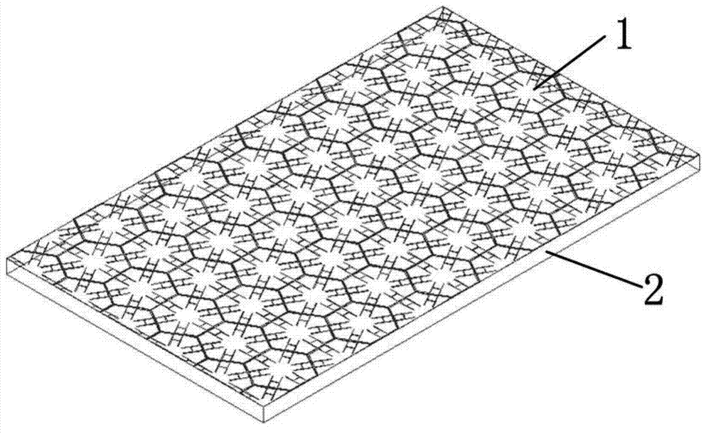
[0030] refer to figure 1 , the present invention includes a metal layer 1 and a dielectric layer 2, the metal layer is located on the upper surface of the dielectric layer, and is composed of a single-layer copper clad laminate. N hexagonal units 11 are etched on the metal layer, these hexagonal units are periodically arranged in a triangular grid, and the distance between the centers of adjacent units is 0.155 times the wavelength corresponding to the central frequency. The dielectric layer adopts an organic polymer substrate with a relative dielectric constant of 2.65, a thickness of 1mm, and N≥3.
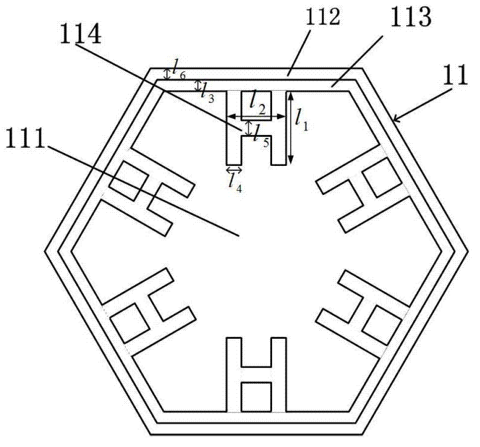
[0031] refer to figure 2 , each hexagonal unit 11 includes a regular hexagonal patch 111 and a regular hexagonal metal wire frame 112, a regular hexagonal gap 113 is provided between the metal patch 111 and the metal wire frame 112, and the width of the regular hexagonal gap is l3 The value is 0.2mm. The perimeter of a regular hexagonal metal wire frame is 46λ / 100, and the wi...
Embodiment 2
[0035] refer to figure 1 , the present invention is composed of a single-layer copper clad laminate, including a metal layer 1 and a dielectric layer 2, and the metal layer is located on the upper surface of the dielectric layer. The dielectric layer adopts an organic polymer substrate with a relative dielectric constant of 4.4 and a thickness of 1 mm. N hexagonal units 11 are etched on the metal layer, these hexagonal units are periodically arranged in a triangular grid, and the distance between the centers of adjacent units is 0.12 times the wavelength corresponding to the center frequency, N≥3.
[0036] refer to figure 2 , each hexagonal unit 11 includes a regular hexagonal patch 111 and a regular hexagonal metal wire frame 112, the perimeter of the regular hexagonal metal wire frame is 36λ / 100, and the wire frame width is l 6 is 0.1 mm, a regular hexagonal gap 113 is provided between the metal patch 111 and the metal wire frame 112, and the width of the regular hexagona...
Embodiment 3
[0038]The structure of this example is the same as that of Example 1. Its different structural parameters are as follows:
[0039] The dielectric layer adopts an organic polymer substrate with a relative permittivity of 3.27. There are 93 hexagonal units 11 etched on the metal layer. These hexagonal units are arranged periodically in a triangular grid, and are relatively The distance between the centers of adjacent hexagonal units is 0.18 times the wavelength corresponding to the center frequency.
[0040] The perimeter of the regular hexagonal metal wire frame of each hexagonal unit is 54λ / 100, and the regular hexagonal gap width l 3 0.5mm, wire frame width l 6 0.5mm.
PUM
 Abstract
Description
Claims
Application Information


