Adhesive composition, method for manufacturing semiconductor device, and semiconductor device

A manufacturing method and semiconductor technology, applied in semiconductor/solid-state device manufacturing, semiconductor devices, semiconductor/solid-state device components, etc., can solve the problems of narrowing the gap between semiconductor chips and substrates, long-term productivity, and inability to inject, and achieve connection Excellent reliability and insulation reliability, improved electrical conductivity, and improved reflow resistance

Active Publication Date: 2013-07-24
RESONAC CORP
View PDF10 Cites 5 Cited by
  • Summary
  • Abstract
  • Description
  • Claims
  • Application Information

AI Technical Summary

Problems solved by technology

With regard to these sealing methods, the gap between the semiconductor chip and the substrate has been narrowed with the progress of miniaturization of semiconductor devices in recent years. Therefore, in the capillary flow method, it takes a long time to inject and lowers the productivity. In the case of injection, even if injection is possible, there are cases where the unfilled part becomes the cause of pores

Method used


Image

  • Adhesive composition, method for manufacturing semiconductor device, and semiconductor device
  • Adhesive composition, method for manufacturing semiconductor device, and semiconductor device
  • Adhesive composition, method for manufacturing semiconductor device, and semiconductor device

Examples


Embodiment 1

[0217] 100 parts by mass of epoxy resin (EP1032), 7.5 parts by mass of curing agent (2PHZ), 175 parts by mass of filler (SM silica), 25 parts by mass of flux activator (diphenolic acid) and MEK solvent according to the solid content of 60 Feed in the form of mass %, add microbeads with a diameter of 0.8 mm and microbeads with a diameter of 2.0 mm in the same amount as the solid content, and stir using a bead mill (Fritsch Japan Co., Ltd., planetary fine pulverizer "P-7") 30 minutes. Next, after adding 100 mass parts of polyimide A (in terms of solid content), and stirring again for 30 minutes by the bead mill, the beads used for stirring were removed by filtration, and the resin varnish was obtained.

[0218] The obtained resin varnish was coated on a substrate film (manufactured by Teijin DuPont Film Co., Ltd., trade name "PUREX A53") using a small precision coating device (Yashii Seiki Co., Ltd.), and placed in a clean oven (manufactured by ESPEC Co., Ltd.). , and dried at ...

Embodiment 2~3 and comparative example 1~6

[0220] Except having changed the composition of the raw material used like following Table 1, it carried out similarly to Example 1, and produced the film adhesive of Examples 2-3 and Comparative Examples 1-6.

[0221] Hereinafter, the evaluation method of the film adhesive obtained by the Example and the comparative example is shown.

[0222]

[0223] The film-like adhesive was cut to a predetermined size (length: 37 mm×width: 4 mm×thickness: 0.13 mm), and was cured by holding at 180° C. for 3 hours in a clean oven (manufactured by ESPEC Corporation). After curing, the elastic modulus at 260° C., which is the reaching temperature of the reflow oven at the time of reflow resistance evaluation, was measured using a viscoelasticity measuring device (manufactured by Rheometrics, trade name “RASII”). The measurement was carried out at a temperature range of -30°C to 270°C, a heating rate of 5°C / min, and a measurement wavelength of 10Hz.

[0224]


PUM

PropertyMeasurementUnit
glass transition temperatureaaaaaaaaaa
particle sizeaaaaaaaaaa
glass transition temperatureaaaaaaaaaa

Abstract

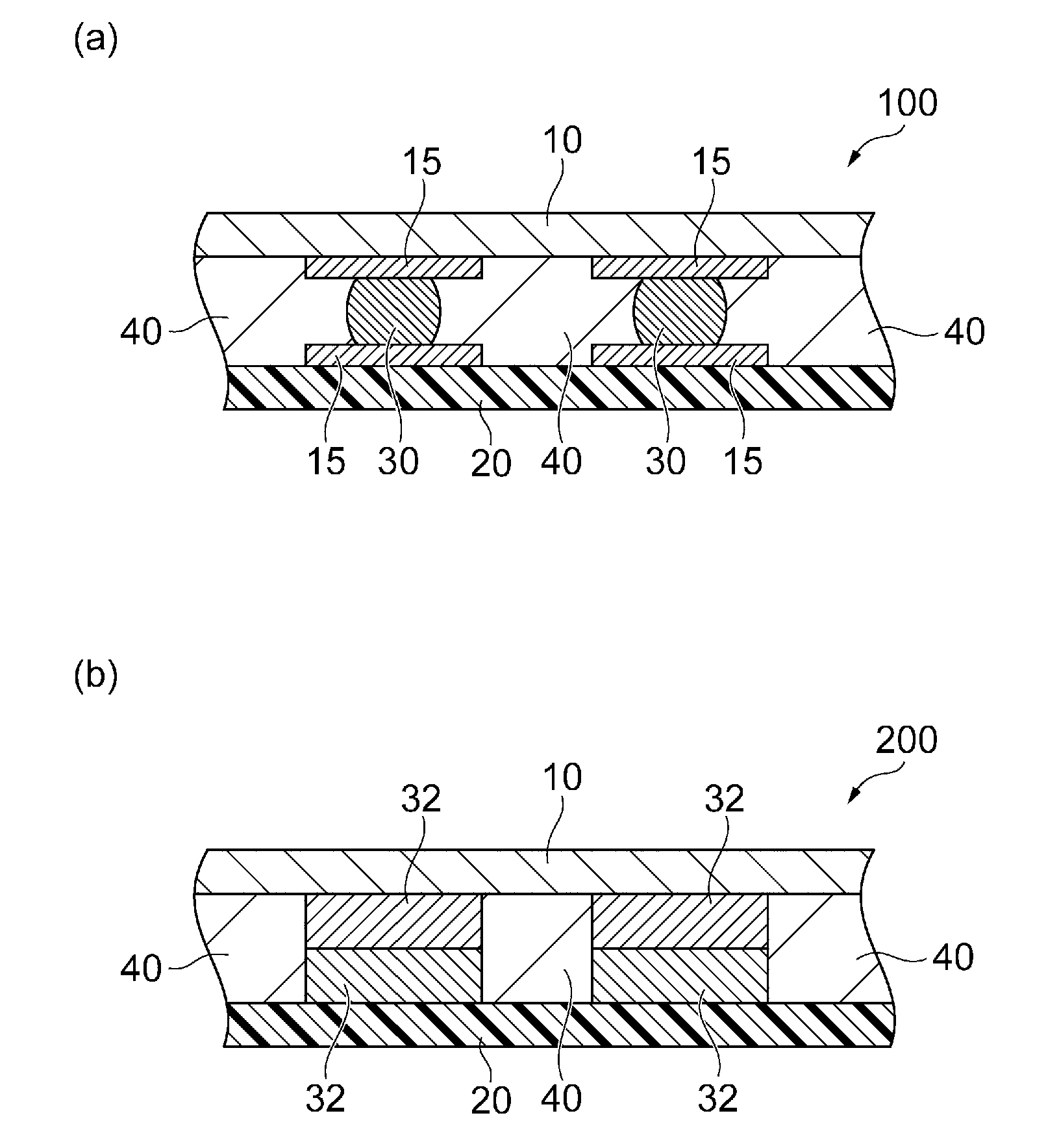
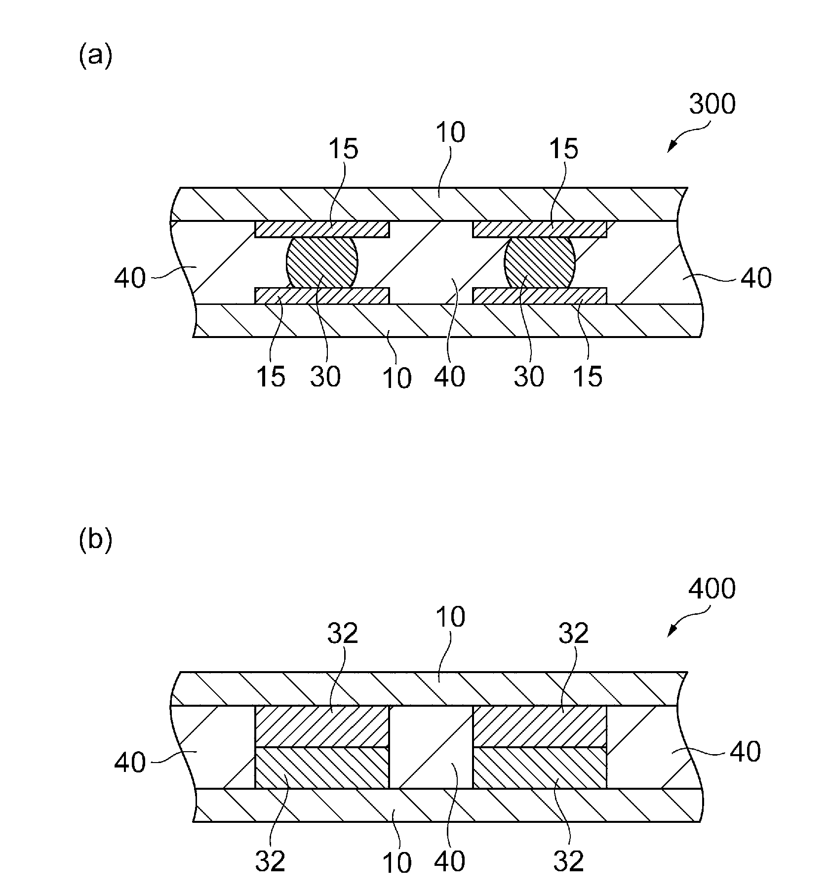
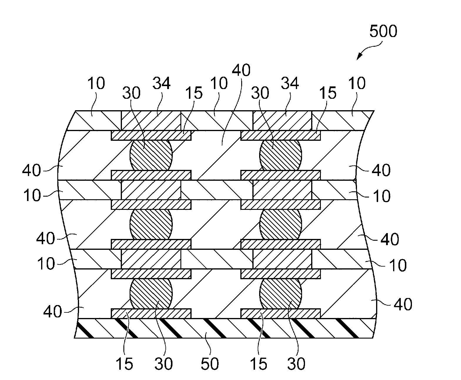
The present invention relates to an adhesive composition for encapsulating connection parts in a semiconductor device in which respective connection parts of a semiconductor chip and a wiring circuit board are electrically connected with each other or alternatively in a semiconductor device in which respective connection parts of a plurality of semiconductor chips are electrically connected with each other. The adhesive composition contains an epoxy resin, a curing agent and an acrylic surface-treated filler.

Description

technical field [0001] The present invention relates to an adhesive composition, a method for manufacturing a semiconductor device, and a semiconductor device. Background technique [0002] In recent years, in order to mount and connect a semiconductor chip to a substrate, a wire bonding method using thin metal wires such as gold wires has been widely used. On the other hand, in order to meet the requirements for miniaturization, thinning, high function, high integration, and high speed of semiconductor devices, conductive protrusions called bumps are formed between the semiconductor chip and the substrate to connect the semiconductor chip and the substrate. The flip-chip connection method (FC connection method) for connection continues to expand. [0003] For example, the COB (Chip On Board) type connection method actively used in BGA (Ball Grid Array) and CSP (Chip Size Package) is also equivalent to the FC connection method for the connection between semiconductor chips ...

Claims


Application Information

Patent Timeline
Patent Type & Authority Applications(China)
IPC IPC(8): H01L21/60C09J7/00C09J11/04C09J11/06C09J163/00H01L23/29H01L23/31H01L25/065H01L25/07H01L25/18
CPCH01L2224/16227H01L2224/13139H01L2924/10329H01L24/29H01L2224/05644H01L24/06H01L2224/05647H01L24/04H01L2224/05571H01L2224/13144H01L24/05H01L2224/13116H01L24/16H01L2224/29298H01L2224/73104H01L2224/16146H01L24/73H01L2224/13155H01L24/13H01L2224/291H01L2225/06565H01L2224/13147H01L2224/2919H01L2224/06181H01L2224/83191H01L2224/05655H01L25/50H01L2924/01012H01L2924/10335H01L2224/16225H01L2924/0665H01L2224/83862H01L2224/13111C09J163/00H01L24/83H01L2224/0557H01L2224/1148C08K9/04H01L2224/9211H01L25/0657H01L2924/0105H01L2924/00011H01L24/92H01L2924/00013H01L2924/01047H01L2924/01006H01L2224/81815H01L2224/05611H01L2924/01079H01L24/11H01L2924/10253H01L2224/05639H01L2924/01082H01L2225/06517H01L2224/05616H01L2225/06541H01L2224/29H01L2224/0401H01L2924/01029H01L2225/06513H01L24/27H01L24/81H01L2924/00014H01L2924/351H01L2924/00C08K9/00H01L2224/29099H01L2224/29199H01L2224/29299H01L2224/2929H01L2224/05552C09J7/00C09J11/06H01L21/56
Inventor 本田一尊永井朗榎本哲也
Owner RESONAC CORP
Why Eureka
Try Eureka