Manufacturing method of imaging nano particle self assembly

A nanoparticle and manufacturing method technology, applied in nanotechnology, semiconductor/solid-state device manufacturing, electrical components, etc., can solve problems such as difficult patterning, limited scope of application, poor controllability, etc., achieve simple operation, improve application range, The effect of convenient batch and parallel processing

Active Publication Date: 2013-07-31
PEKING UNIV
View PDF3 Cites 4 Cited by
  • Summary
  • Abstract
  • Description
  • Claims
  • Application Information

AI Technical Summary

Problems solved by technology

However, since the substrate used is a single crystal silicon wafer with single-sided polishing and no other structures on the surface, the prepared nanoparticle close-packed structure is distributed on the entire substrate surface without specific patterns.
Therefore, this self-assembly method is less controllable, difficult to pattern, and limited in scope

Method used


Image

  • Manufacturing method of imaging nano particle self assembly
  • Manufacturing method of imaging nano particle self assembly
  • Manufacturing method of imaging nano particle self assembly

Examples


Embodiment Construction

[0021] The present invention will be described in detail below in conjunction with the accompanying drawings and embodiments.

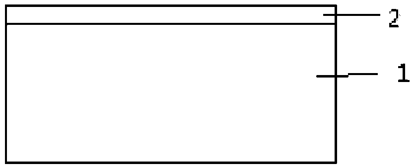
[0022] 1) if figure 1 As shown, a 4-inch single-sided polished single-crystal silicon substrate 1 is prepared, and a layer of parylene (Parylene) film 2 is deposited on the surface of the silicon substrate 1 by chemical vapor deposition (Chemical Vapor Deposition-CVD).

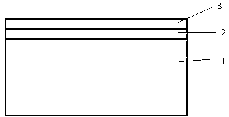
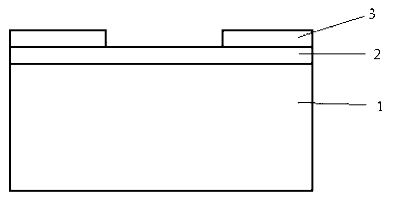
[0023] 2) As shown in Figure 2, by traditional photolithography method, on silicon substrate 1 surface, spin-coat photoresist 3 mask (such as Figure 2a shown), and then according to the production sequence of glue rejection, pre-baking, exposure, post-baking and developing, the required photoresist 3 mask pattern is made on the surface of the silicon substrate 1 (such as Figure 2b shown);

[0024] Wherein, the mask thickness of the photoresist 3 is 1.0 μm˜2.0 μm.

[0025] 3) if image 3 As shown, the exposed parylene film 2 is etched by an oxygen plasma etching method.

[0026]...


PUM

PropertyMeasurementUnit
thicknessaaaaaaaaaa
thicknessaaaaaaaaaa

Abstract

The invention relates to a manufacturing method of imaging nano particle self assembly, which comprises the steps of adopting a one-side polishing single-crystal silicon substrate, depositing a poly-p-xylylene membrane on the surface of the silicon substrate by a chemical vapor deposition method, fabricating a required photoresist mask pattern on the surface of the silicon substrate by the traditional photoetching method, etching the exposed poly-p-xylylene membrane by adopting an oxygen plasma etching method, using a diamond scribing machine to scribe the silicon substrate, using acetone to remove a photoresist on the surface of the silicon substrate, soaking the silicon substrate after the photoresist is removed in mixed liquid of concentrated sulfuric acid and hydrogen peroxide, taking out the silicon substrate, using deionized water to clean the silicon substrate, taking a certain amount of prepared nano particle suspension liquid to drop into a container containing ethanol, uniformly mixing the two liquid, slowly pouring into a culture dish containing the deionized water, completely soaking the obtained silicon substrate in the liquid in the culture dish, taking the silicon substrate out, placing the silicon substrate in another culture dish, horizontally placing the silicon substrate in a drying oven, and obtaining the silicon substrate with the imaging nano particle self assembly after natural evaporation at a room temperature.

Description

technical field [0001] The invention relates to a method for manufacturing patterned nanoparticle self-assembly, in particular to a method for preparing a hydrophilic-hydrophobic silicon substrate to assist nanoparticle self-assembly by utilizing the self-assembly phenomenon induced by nanoparticle evaporation. Background technique [0002] Self-assembly (self-assembly) refers to the process in which structural units such as molecules and nanoparticles spontaneously associate into thermodynamically stable, structurally determined, and special-performance aggregates through non-covalent bonds under equilibrium conditions. The biggest feature of self-assembly is that once the self-assembly process starts, it will automatically proceed to a certain expected end point, and the structural units such as molecules will be automatically arranged into an orderly pattern, and no external force is required even to form a complex functional system. Self-assembly can form monolayers, mem...

Claims


Application Information

Patent Timeline
Patent Type & Authority Applications(China)
IPC IPC(8): H01L21/02B82Y40/00
Inventor 吴文刚杨增飞钱闯王诣斐
Owner PEKING UNIV
Why Eureka
Try Eureka