Crystalline silicon and preparation method thereof

A technology of crystalline silicon and monocrystalline silicon, applied in the field of crystalline silicon and its preparation, can solve the problems of accumulation of dislocations, high cost of casting monocrystalline silicon wafers, and low conversion efficiency.

Active Publication Date: 2013-08-21
JIANGSU XIEXIN SILICON MATERIAL TECH DEV
View PDF2 Cites 5 Cited by
  • Summary
  • Abstract
  • Description
  • Claims
  • Application Information

AI Technical Summary

Problems solved by technology

However, affected by the nucleation of the crucible wall and the solid-liquid interface during crystal growth, polycrystalline nucleation occurs in the silicon ingot near the crucible surface, and a large number of dislocations accumulate, resulting in a silicon wafer in which polycrystalline and single crystal interact. , the conversion efficiency of these edge silicon wafers is low, even lower than that of ordinary polycrystalline silicon wafers
At the same time, due to the high production cost of monocrystalline silicon seed crystals in monocrystalline silicon, the cost of cast monocrystalline silicon wafers is higher than that of ordinary polycrystalline silicon wafers, which seriously restricts the mass production of cast monocrystalline silicon wafers

Method used


Image

  • Crystalline silicon and preparation method thereof
  • Crystalline silicon and preparation method thereof
  • Crystalline silicon and preparation method thereof

Examples


preparation example Construction

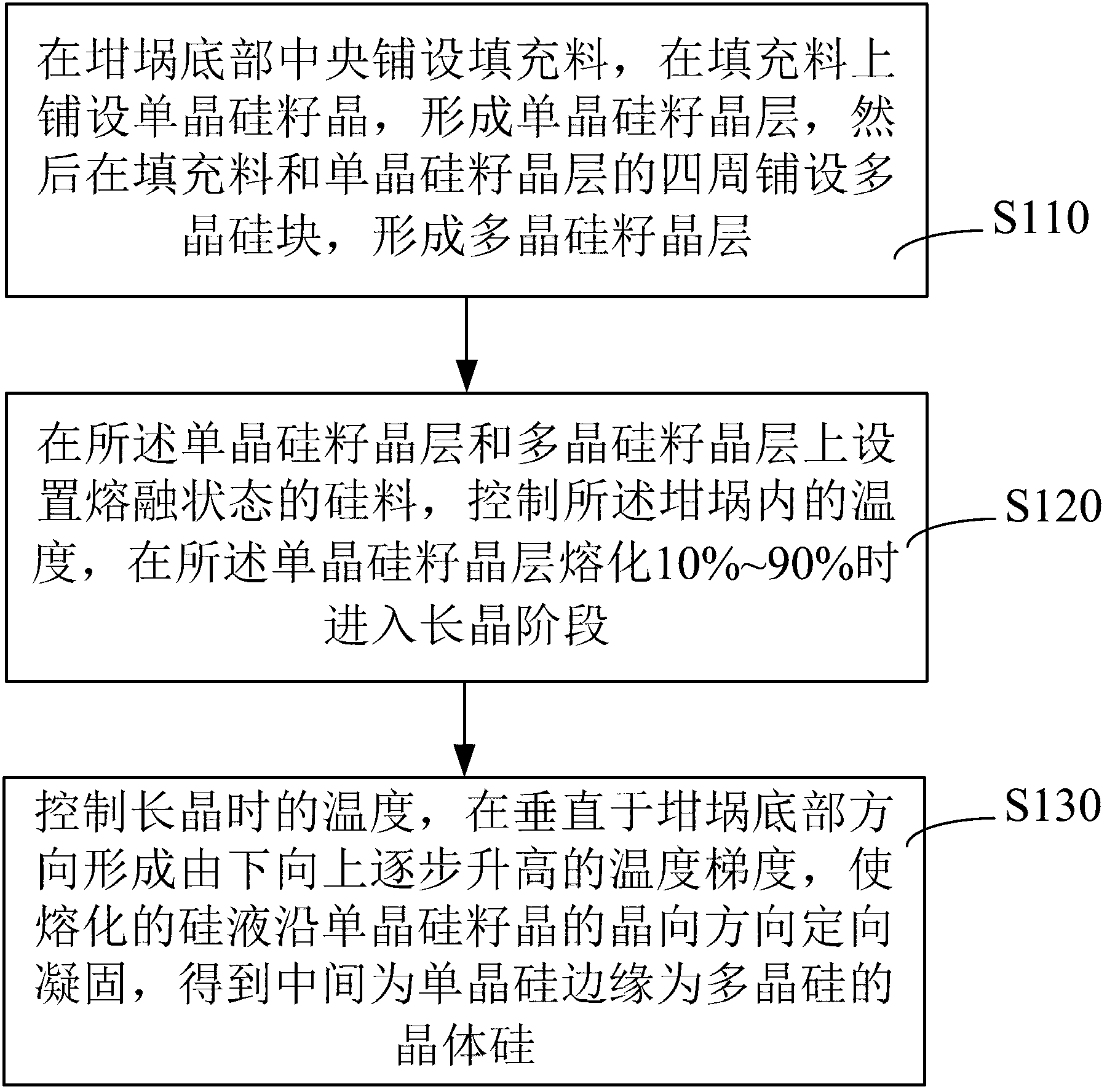
[0019] Please refer to figure 1 and figure 2 , a method for preparing crystalline silicon according to one embodiment, comprising the following steps.

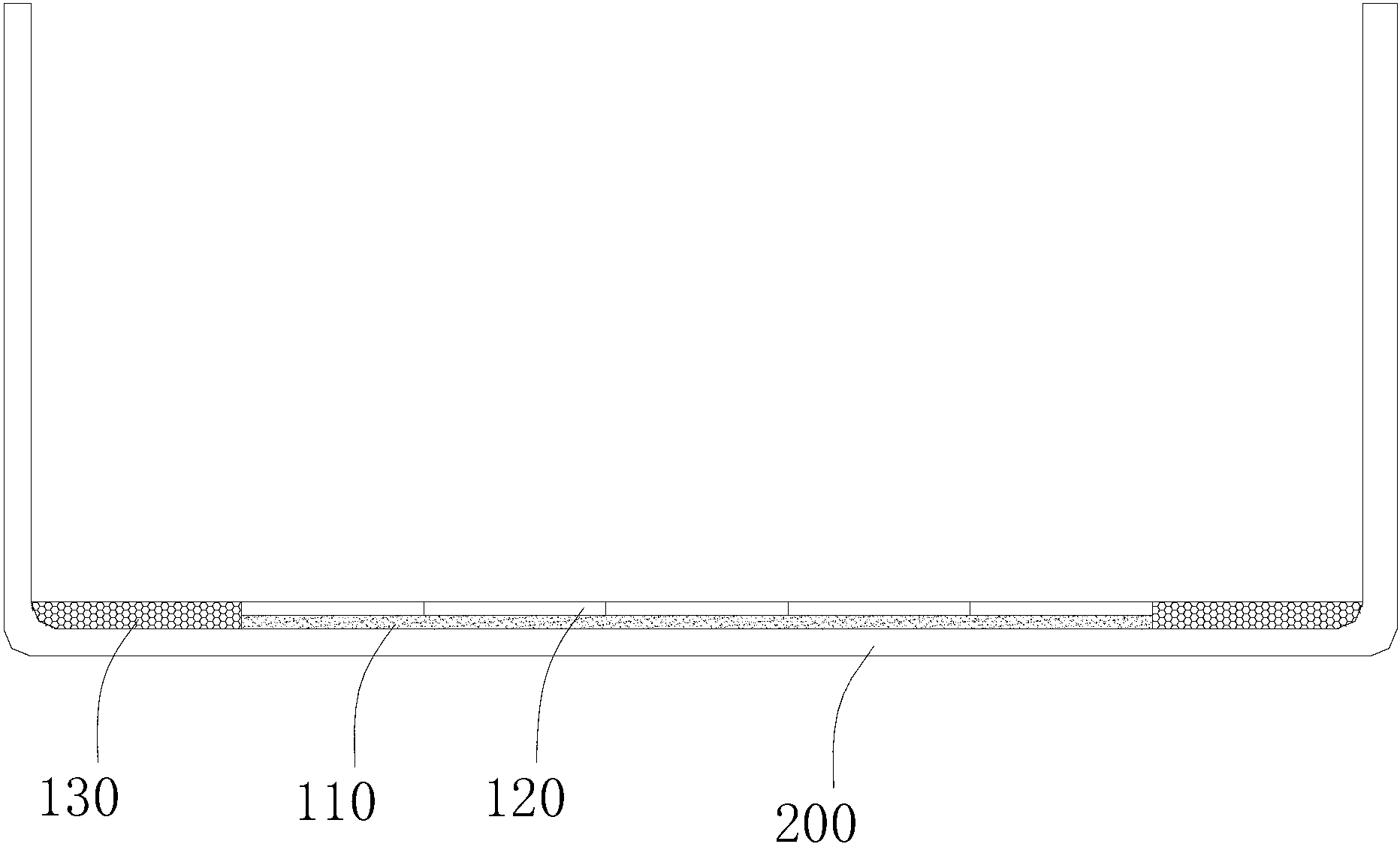
[0020] Step S110, laying a filling material in the center of the bottom of the crucible, laying a monocrystalline silicon seed crystal on the filling material to form a monocrystalline silicon seed crystal layer, and then laying polycrystalline silicon blocks around the filling material and the monocrystalline silicon seed crystal layer to form a polycrystalline silicon seed crystal layer.

[0021] Please refer to figure 2 , in the center of the bottom of the crucible 200, the filling material 110 is first laid, and then the single crystal silicon seed crystal is laid on the filling material 110 to form the single crystal silicon seed crystal layer 120, and then the filling material 110 and the single crystal silicon seed crystal layer 120 A polysilicon block is laid around to form a polysilicon seed crystal layer 130 . ...

Embodiment 1

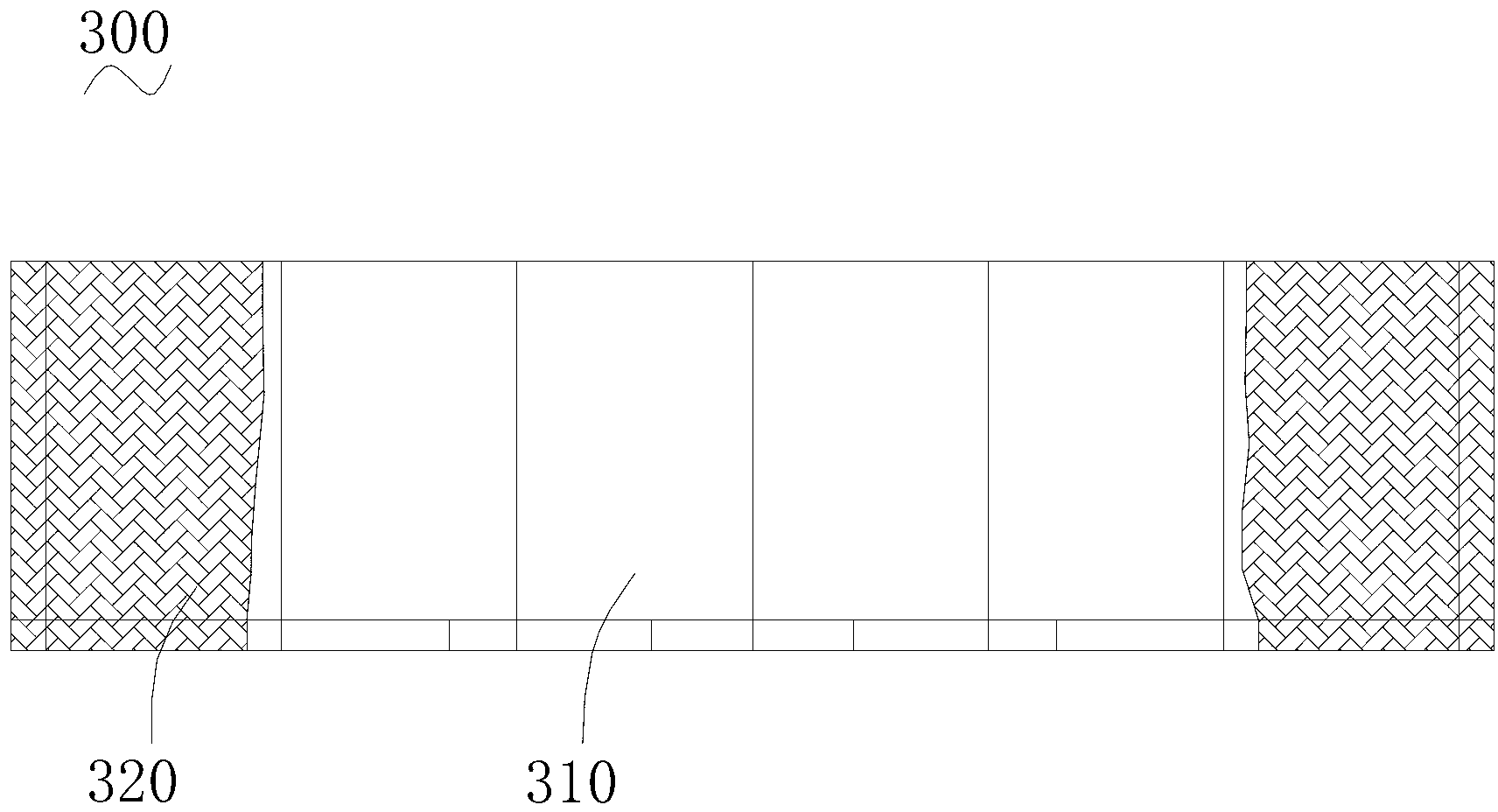
[0033] like figure 2 As shown, the filler is laid in the center of the bottom of the crucible, the monocrystalline silicon seed crystal is laid on the filler to form a monocrystalline silicon seed layer, and the polycrystalline silicon block is laid around the monocrystalline silicon seed layer and the filler to form a polycrystalline silicon seed layer. The filling material is silicon powder, and the thickness is 15mm. The size of the monocrystalline silicon seed crystal is 160×160×15mm, and there are 9 pieces in total, which are closely arranged in 3×3. The size of the polycrystalline silicon blocks laid around the monocrystalline silicon seed crystal is 140×140×25 mm.

[0034] Setting the silicon material in molten state on the monocrystalline silicon seed crystal layer and the polycrystalline silicon seed crystal layer is as follows: put 500 kg of polycrystalline silicon material on the polycrystalline silicon seed crystal layer and the monocrystalline silicon seed cryst...

Embodiment 2

[0036] like figure 2 As shown, the filler is laid in the center of the bottom of the crucible, the monocrystalline silicon seed crystal is laid on the filler to form a monocrystalline silicon seed layer, and the polycrystalline silicon block is laid around the monocrystalline silicon seed layer and the filler to form a polycrystalline silicon seed layer. Among them, the filling material is a silicon block with a size of 156×156×10mm, a total of 9 pieces, which are closely arranged in 3×3 at the bottom of the crucible. The size of the monocrystalline silicon seed crystal is 120×120×10mm, and there are 16 pieces in total, which are closely arranged in 4×4. The size of the polycrystalline silicon blocks laid around the monocrystalline silicon seed crystal is 156×156×20 mm.

[0037] Setting the silicon material in molten state on the monocrystalline silicon seed crystal layer and the polycrystalline silicon seed crystal layer is as follows: put 450 kg of polycrystalline silicon ma...


PUM

PropertyMeasurementUnit
thicknessaaaaaaaaaa
thicknessaaaaaaaaaa
thicknessaaaaaaaaaa

Abstract

The invention relates to a preparation method of crystalline silicon. The preparation method comprises the following steps: laying a filling material at the center of the bottom of a crucible, laying monocrystalline silicon seeds on the filling material to form a monocrystalline silicon seed layer, and laying polycrystalline silicon blocks at the periphery of the filling material and the monocrystalline silicon seed layer to form a polycrystalline silicon seed layer; arranging a silicon material in a molten state on the monocrystalline silicon seed layer and the polycrystalline silicon seed layer, controlling the temperature in the crucible and entering into a crystal growth stage when 10%-90% of the monocrystalline silicon seed layer is molten; and controlling the temperature during crystal growth, forming a temperature gradient which is gradually increased from bottom to top in the direction which is vertical to the bottom of the crucible, and solidifying molten silicon liquid in the fixed direction along the crystal direction of the monocrystalline silicon seed to get the crystalline silicon with monocrystalline silicon at the middle part and polycrystalline silicon at the edge. By adopting the method, the using quantity of the monocrystalline silicon seed is reduced, and the conversion efficiency of an edge silicon chip is improved. The invention further provides the crystalline silicon prepared through the method.

Description

technical field [0001] The invention relates to the field of solar photovoltaic material preparation, in particular to crystalline silicon and a preparation method thereof. Background technique [0002] Solar photovoltaic power generation is one of the fastest-growing forms of sustainable energy utilization, and it has developed rapidly in various countries in recent years. At present, the method of producing monocrystalline silicon for solar energy by casting method has received more and more attention. Cast single crystal silicon has the advantages of low defects of Czochralski single crystal silicon, and can form a pyramid-shaped texture by alkali texturing method, which can improve the absorption of light, thereby improving the conversion efficiency; at the same time, cast single crystal silicon also has the advantages of casting Polysilicon has the advantages of low production cost and high output. Therefore, cast monocrystalline silicon inherits the advantages of Czo...

Claims


Application Information

Patent Timeline
Patent Type & Authority Applications(China)
IPC IPC(8): C30B11/14C30B28/06C30B29/06
Inventor 武鹏胡亚兰游达郑玉芹徐岩郑循强
Owner JIANGSU XIEXIN SILICON MATERIAL TECH DEV
Why Eureka
Try Eureka